At the 2024 GTC conference, NVIDIA unveiled its groundbreaking Blackwell AI chip. What sets it apart, and what insurmountable barriers does it overcome?
Before diving into the specifics of Blackwell, let’s gain a high-level understanding of the GB200 design philosophy. GB200 represents NVIDIA’s most powerful AI superchip, potentially forming the backbone of the world’s most potent AI servers. How did NVIDIA achieve this feat?
The answer lies in meticulous research and development, coupled with a clear expansion strategy. Jensen Huang (CEO of NVIDIA) revealed that Blackwell’s development cost was approximately $10 billion—a staggering investment.
Now, let’s delve into the five layers of compute power:
Single-Chip Compute Power
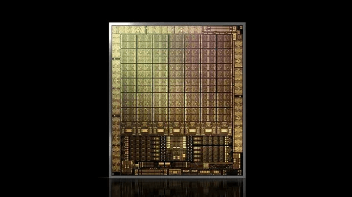
Under the constraints of equivalent process technology, a larger chip area accommodates more transistors. Blackwell’s chip size pushes the limits, spanning an entire wafer (800 mm²) within the maximum exposure limits of lithography machines. Huang humorously quipped that going any larger might cause the entire wafer to fracture due to physical limitations.
Many perceive AI compute power as the accumulation of streaming multiprocessor (SM) cores. While this holds true to some extent, it’s essential to explore the advancements in single-card compute power. For instance, Huawei’s Ascend 910B processor approaches A100 levels by increasing SMs.
However, as we’ll see, single-card compute power represents only the first level of AI capability. Let’s now examine Blackwell’s progress in this domain.
To address this, let’s revisit the historical development of NVIDIA’s AI accelerator cards. The first-generation AI accelerator card, Volta, introduced the Tensor Core architecture specifically designed for AI computations. The GPU V100, based on this architecture, featured 80 SM units, each containing 8 computational cores (blocks). Each core could complete 128 16-bit floating-point multiply-accumulate operations per cycle. With a clock frequency of 1.53 GHz, the V100’s floating-point compute power amounted to 125 teraflops (TFLOPS).
To facilitate everyone’s understanding, let’s briefly explain some of the abbreviations here. “FLOPS” stands for “Floating Point Operations Per Second,” representing the number of floating-point calculations performed per second. “Tera” is a scientific notation unit, where 1 Tera equals 1000 Giga. In this context, “Tera” corresponds to a specific order of magnitude.
Now, let’s delve into the details of NVIDIA’s various GPU architectures:
Turing Architecture (T4):
- The second-generation tensor computing architecture by NVIDIA is called “Turing.” It represents the T4 graphics card.
- A T4 card contains 40 Streaming Multiprocessors (SMs), and other specifications are similar to the V100.
- Consequently, the T4’s computational power is approximately half that of the V100, specifically around 65 TFLOPS.
Ampere Architecture (A100):
- The third-generation tensor processing architecture is Ampere, which includes the familiar A100 series graphics cards.
- With advancements in chip fabrication technology, the A100 features 108 SMs (doubling the previous generation) with the same core count as the V100.
- The upgraded compute units allow each core to perform 256 floating-point multiplications and accumulations per cycle (twice the capability of the older architecture).
- Additionally, the A100 introduces an 8-bit floating-point (FP8) mode optimized for deep learning workloads. Each 16-bit core can function as two 8-bit cores, further boosting computational power.
- Despite a slight decrease in clock frequency (1.41 GHz), the A100 achieves nearly 5 times the computational power of the V100, totaling 624 TFLOPS (FP8).
Hopper Architecture (H100):
- The fourth-generation architecture, known as Hopper, was released by NVIDIA last year.
- Although the number of SMs (132) in the H100 series did not significantly increase compared to the previous generation, it features a novel Tensor Core architecture and asynchronous memory design.
- Each SM core can now perform FP16 multiplications and accumulations 512 times per cycle.
- The clock frequency is slightly higher at 1.83 GHz.
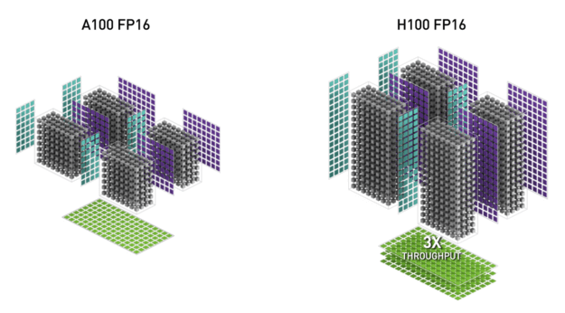
- As a result, a single H100 card achieves an astonishing 1978 Tera FLOPS (FP8), entering the PFLOPS (1.97 Peta FLOPS) domain for the first time.
- To put this in perspective, 1 PFLOPS equals 1000 TFLOPS.
- Imagine expanding your hard drive capacity a thousandfold, and you’d have 1 PB—a common storage unit in large data centers.
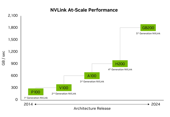
Last week, Huang unveiled the fifth-generation Blackwell architecture, marking significant progress in computational power. Based on publicly available data, the GB200, utilizing the new FP4 data unit, is expected to achieve 20 PetaFLOPS of computational power in inference tasks. When converted back to FP8 precision, it should still deliver an impressive 10 PFLOPS, representing approximately a fivefold improvement over the H100.
Publicly disclosed information indicates that Blackwell operates at a clock frequency of 2.1 GHz. Assuming minimal architectural changes, this implies that Blackwell will feature 600 Streaming Multiprocessors (SMs), nearly four times that of the H100. With two dies in the Blackwell design, even a single-die GPU will have twice the number of SMs as the H100.
The remarkable increase in computational power owes much to advancements in lithography, chip etching, and physical limitations related to wafer size—the first level of improvement. Additionally, NVIDIA’s continuous refinement of the Tensor Core architecture, including optimized pipelines for Transformers and dedicated CUDA drivers, has significantly contributed to Blackwell’s enhanced performance.
However, the fundamental boost in Blackwell’s computational power primarily stems from the increased number of SMs. Compared to the Hopper architecture introduced in 2023, Blackwell achieves approximately a fivefold improvement. When compared to the Volta architecture from 2017, the leap is even more substantial—around 40 times.
The second layer of computational power involves Die-to-Die interconnects.
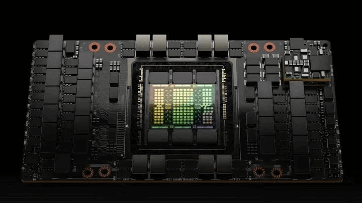
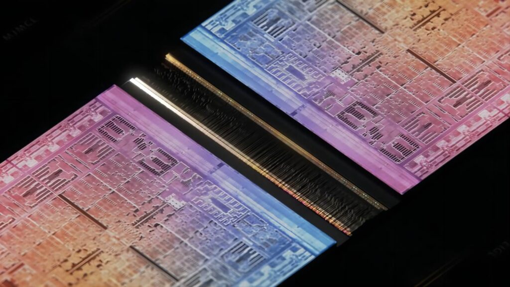
Blackwell achieves 600 SMs by creating the world’s largest chiplet: directly bonding two GPU cores into a massive unit that breaks the physical limitations of a single wafer. The communication speed between these cores reaches a staggering 10 TB/s, leading them to perceive themselves as a colossal single chip.
While the constraints of photomasks, exposure, wafer size, and process dimensions typically limit the number of transistors on a single chip, Blackwell defies these boundaries. Its chip area spans 800 square millimeters, referred to as “Reticle-Sized,” indicating the maximum size producible by photolithography machines.
Huang’s ambition doesn’t stop there. He ventures into the next level of computational power: connecting two dies to form an even larger chiplet. As long as the interconnect speed remains sufficiently fast, these two chiplets will operate as a single unit—the birth of the world’s largest GPU.
Why two chiplets and not three or four? The principle of “one begets two, two begets all things” applies here. “Two” represents the optimal solution for chip communication and complexity within current technological constraints.
Apple also has its own dual-die interconnect technology called UltraFusion, albeit with reduced communication capacity (only 2.5 TB/s). However, Huang Renxun’s GPUs are industrial products, far surpassing consumer-grade electronics.
This achievement is a cost-no-object show of prowess by NVIDIA, driven by explosive demand for computational power. Blackwell boasts the world’s fastest Die-to-Die communication at a staggering 10 TB/s, utilizing a technology called NV-HBI (High Bandwidth Interface), which remains undisclosed. We speculate that it might be a variant of NVLINK 5.0 or 224G XSR serdes, employing 48 channel groups for a total bandwidth of 10 TB/s.
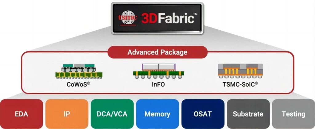
Regardless of the specific technology NVIDIA adopts, this places entirely new demands on Advanced Packaging. Packaging companies, through intricate copper wire threading within the board and metal solder balls on the PCB’s back, achieve complex 2.5D interconnects—a true technical feat. Packaging, second only to photolithography, presents a significant challenge for the domestic chip industry.
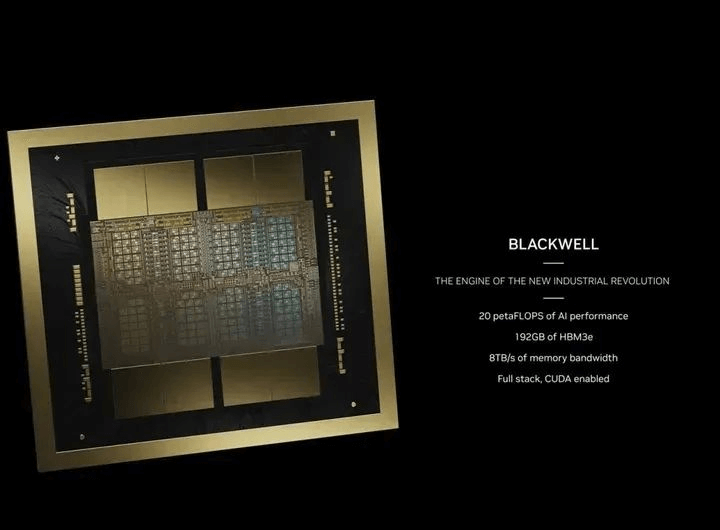
In summary, Blackwell boasts 206 billion transistors, supporting up to eight HBM3e memory stacks (instead of four), each with 24 GB capacity and 1 TB/s bandwidth. Consequently, the B200 GPU will offer a total of 192 GB of memory and 8 TB/s memory bandwidth.
The research and development cost for Blackwell GPUs is a staggering $10 billion. Achieving ultimate single-GPU computational power, this marks the first line of defense for NVIDIA’s AI supercomputing processors.
As for interconnecting three, four, or more GPUs, Huang Renxun leaves that challenge to the next level of computational power: NVLink.
The third tier of computational power in NVIDIA’s Blackwell architecture involves NVLink and interconnects 72 GPUs.
While combining two dies into a single GPU seems powerful, practical applications still require more. For large language models with hundreds of billions of parameters, achieving timely training on massive text corpora with trillions of tokens demands extensive parallel computing.
Data parallelism is one aspect, where model weights and even individual layers must be distributed across different GPUs for parallel computation, achieving three-dimensional divide-and-conquer acceleration. For parallel training of large language models, we can refer to HuggingFace’s insights on this topic.
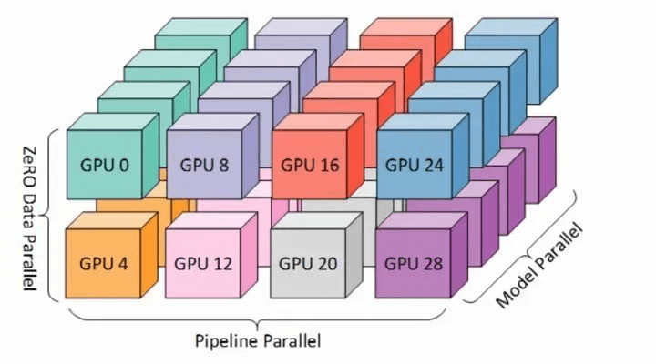
What we need to understand is that even with ample memory, a single GPU falls short for large language model training.
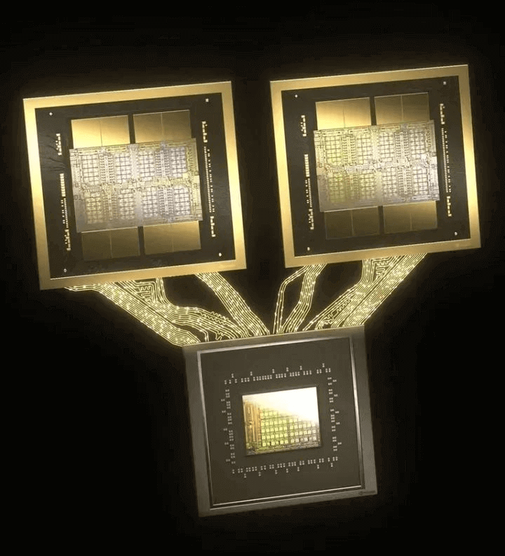
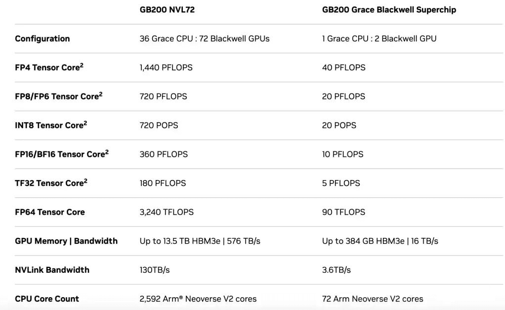
NVIDIA’s solution involves assembling two Blackwell GPUs and an Arm processor (Grace CPU) on a single motherboard. This product, named GB200 (Grace Blackwell 200), boasts two Blackwell GPUs and four dies, resulting in an FP8 computational power of 20 PFLOPS—twice that of a single GPU. The two GPUs are interconnected via NVLink technology, assisted by the Grace CPU, achieving a communication bandwidth of 1.8 TB/s per GPU and a total bandwidth of 3.6 TB/s. The specific connection is illustrated in the diagram below:
Subsequently, NVIDIA assembles 36 such PCB boards (referred to as a rack) into a standard server chassis. These 36 mainboards remain interconnected using NVLink, facilitated by copper cable electrical signals.
Under the NVLink 5 standard, each GPU can communicate with up to 18 other GPUs simultaneously, resulting in a total bandwidth of 1.8 TB/s—14 times that of PCIe 5. In total, the 72 GPUs achieve a combined communication bandwidth of 130 TB/s, which could theoretically accommodate the entire internet.
This cabinet, equipped with 72 Blackwell GPU cores, is named GB200 NVL72. The 72-GPU interconnect surpasses traditional 8-GPU parallel schemes (such as those from Huawei and AMD) by a factor of 9. NVL72’s configurable high-speed HBM3e memory capacity increases from the single-card 192 GB to a whopping 13.5 TB, with a maximum memory bandwidth of 576 TB/s.
These numbers may seem dizzying, but their impact on large model training speed is undeniable. Compared to the GB200 with only two GPUs, the NVL72’s performance improvement is a staggering 36-fold. We’ve truly entered the realm of supercomputing, where simplicity meets brute force.
Specifically, GB200 NVL72 achieves 720 PFLOPS in FP8 computational power and, for the first time, enters the Exa realm with 1.44 Exa FLOPS in FP4. This explains why, in inference tasks, NVL72 outperforms the H100 by up to 30 times.
Exascale computational power now rivals the world’s top supercomputers. While supercomputers achieve this level of performance using FP64 calculations and millions of CPU cores, GB200 NVL72 accomplishes it with just 72 GPUs
Fourth Layer Computing: NVSwitch, SuperPOD
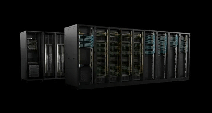
When one cabinet isn’t enough, the solution is to add more cabinets. This straightforward, brute-force approach is the fundamental principle behind Jensen Huang’s Scale Up supercomputing strategy.
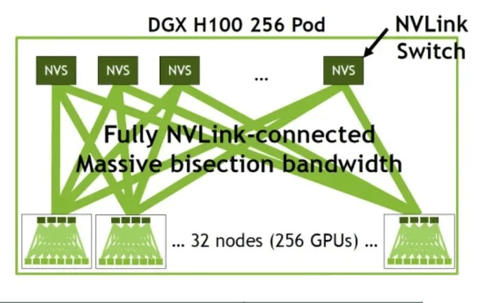
In theory, leveraging NVSwitch allows for a maximum of 576 GPU connections via NVLink. Coincidentally, this aligns with the configuration of 8 GB200-NVL72 cabinets, which NVIDIA refers to as GB200 SuperPOD.
Each NVSwitch provides up to 144 NVLink interfaces. Within a single cabinet, you would need 9 NVSwitches, resulting in 72 GPUs—each fully loaded with 18 NVLink connections (72 * 18 = 9 * 144).
NVLink offers an All-to-All GPU connection, meaning each GPU has both upstream and downstream channels, connecting to any other GPU within the system.
NVLink 5 has a significant advantage over the previous GH100 product: while the older generation allowed a maximum of 64 NVLink channels per NVSwitch and 256 GPUs in an NVLINK system, GB200 can accommodate 72 GPUs in a single cabinet (6 H100s). For 256 GPUs across 8 cabinets, you’d need a total of 72 NVSwitches (9 * 8).
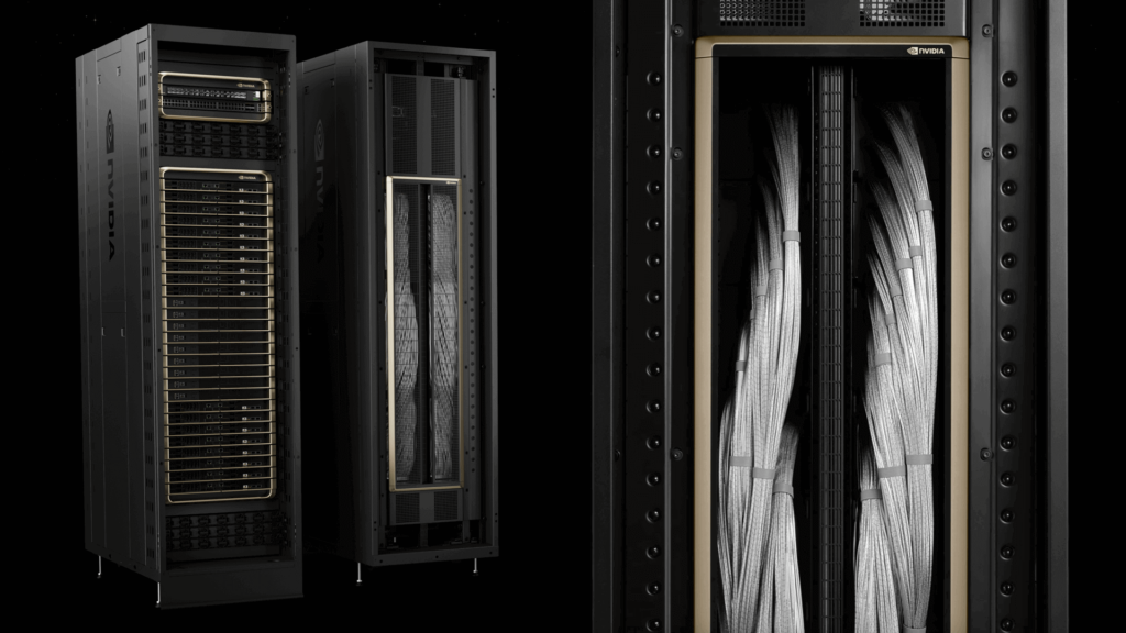
Between cabinets, NVIDIA’s ConnectX series network cards, using InfiniBand standards, connect via Ethernet at 400 GB/s. This explains the blue cables visible on the rear side of the depicted setup. An 800G OSFP typically supports either 2 channels at 400 GB/s or 8 channels at 100 GB/s.
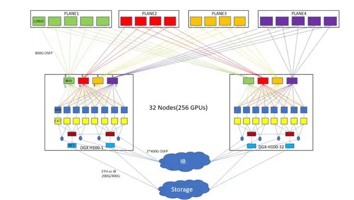
Alternatively, an unconventional approach involves using NVSwitches for interconnecting the outermost cabinets, as shown below. In this configuration, 8 H100s form a node, resulting in 32 nodes. Each node internally connects using 4 NVSwitches. Following the arrangement of the fiber switches in the diagram, an additional 18 NVSwitches are used to fully connect the spare interfaces in each node. This totals 146 NVSwitches.
While NVSwitch’s maximum aggregate bandwidth is 1 PB/s (nearly 500 times that of a single NVLink), its peak non-blocking bandwidth of 14.4 TB/s falls far short of the 130 TB/s within a single NVL72 cabinet. Therefore, performance scaling is not lossless. During training, communication tasks should primarily occur within cabinets, with inter-cabinet communication reserved for specific needs, such as gradient updates after completing a batch.
Without a doubt, if you can afford these 8 cabinets, your computational power (FP4 calculations) would reach an astounding 11.52 Exa FLOPS. Even for commonly used FP8, that’s 5.76 Exa FLOPS. Impressive, isn’t it?
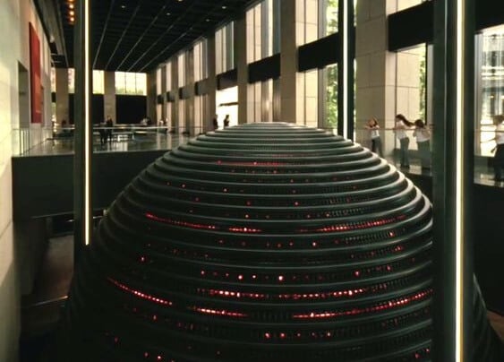
Fifth Layer Computing: AI Super Factory
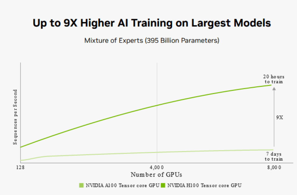
At the previous GTC conference in 2023, Huang unveiled an intriguing image: a system capable of supporting 8,000 GPUs, completing the training of a massive 400-billion-parameter MoE hybrid expert language model in just 20 hours—a task that would have taken three months otherwise. NVIDIA is likely collaborating with cloud providers like Azure, and it’s safe to assume that this system is a one-of-a-kind global phenomenon.
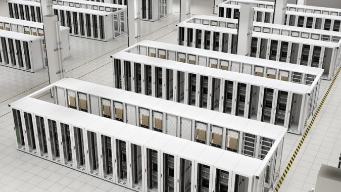
The vast number of GPUs likely interconnects across multiple SuperPODs using optical switches and fiber topology. The entire data center will become a GPU-dominated realm. In the future, alongside nuclear power plants, we may witness the rise of computational factories—much like the prophetic Rehoboam from the TV series “Westworld.” These factories will create AGI (Artificial General Intelligence) and potentially rule the human world.
Below, you’ll find a conceptual diagram of the computational factory, followed by an image of Rehoboam:
As for computational power? If you’re still curious, consider this: with 8,000 GPUs (20 times the SuperPOD estimate), FP4 calculations would reach an unprecedented 220 Exa FLOPS. Even for commonly used FP8, we’re looking at 115 Exa FLOPS.
Related Products:
-
 NVIDIA MMA4Z00-NS400 Compatible 400G OSFP SR4 Flat Top PAM4 850nm 30m on OM3/50m on OM4 MTP/MPO-12 Multimode FEC Optical Transceiver Module
$550.00
NVIDIA MMA4Z00-NS400 Compatible 400G OSFP SR4 Flat Top PAM4 850nm 30m on OM3/50m on OM4 MTP/MPO-12 Multimode FEC Optical Transceiver Module
$550.00
-
NVIDIA MMA4Z00-NS-FLT Compatible 800Gb/s Twin-port OSFP 2x400G SR8 PAM4 850nm 100m DOM Dual MPO-12 MMF Optical Transceiver Module
$650.00
-
NVIDIA MMA4Z00-NS Compatible 800Gb/s Twin-port OSFP 2x400G SR8 PAM4 850nm 100m DOM Dual MPO-12 MMF Optical Transceiver Module
$650.00
-
NVIDIA MMS4X00-NM Compatible 800Gb/s Twin-port OSFP 2x400G PAM4 1310nm 500m DOM Dual MTP/MPO-12 SMF Optical Transceiver Module
$900.00
-
NVIDIA MMS4X00-NM-FLT Compatible 800G Twin-port OSFP 2x400G Flat Top PAM4 1310nm 500m DOM Dual MTP/MPO-12 SMF Optical Transceiver Module
$1199.00
-
NVIDIA MMS4X00-NS400 Compatible 400G OSFP DR4 Flat Top PAM4 1310nm MTP/MPO-12 500m SMF FEC Optical Transceiver Module
$700.00
-
NVIDIA(Mellanox) MMA1T00-HS Compatible 200G Infiniband HDR QSFP56 SR4 850nm 100m MPO-12 APC OM3/OM4 FEC PAM4 Optical Transceiver Module
$139.00
-
NVIDIA MFP7E10-N010 Compatible 10m (33ft) 8 Fibers Low Insertion Loss Female to Female MPO Trunk Cable Polarity B APC to APC LSZH Multimode OM3 50/125
$47.00
-
NVIDIA MCP7Y00-N003-FLT Compatible 3m (10ft) 800G Twin-port OSFP to 2x400G Flat Top OSFP InfiniBand NDR Breakout DAC
$260.00
-
NVIDIA MCP7Y70-H002 Compatible 2m (7ft) 400G Twin-port 2x200G OSFP to 4x100G QSFP56 Passive Breakout Direct Attach Copper Cable
$155.00
-
NVIDIA MCA4J80-N003-FTF Compatible 3m (10ft) 800G Twin-port 2x400G OSFP to 2x400G OSFP InfiniBand NDR Active Copper Cable, Flat top on one end and Finned top on other
$600.00
-
NVIDIA MCP7Y10-N002 Compatible 2m (7ft) 800G InfiniBand NDR Twin-port OSFP to 2x400G QSFP112 Breakout DAC
$190.00