
Introduction
Data Center Networks (DCNs) face challenges due to the exponential growth in data traffic driven by applications such as video streaming, artificial intelligence, machine learning, and cloud computing. Traditional electronic switches struggle to keep up with growing bandwidth and connectivity demands while maintaining low power consumption and low latency. Optical switch technology offers a promising solution to these challenges by providing high-bandwidth, low-latency, and energy-efficient switching.
This article provides an overview of optical switch architectures for next-generation data center and high-performance computing (HPC) networks. We will present key performance metric, switch architectures, integrated optical switch technology, and example implementations. Finally, we will discuss the challenges and future prospects of optical switches in data centers.
Key Performance Metric
When evaluating optical switches for data center applications, several key metrics must be considered:
- Capacity: High-bandwidth switching is required, especially for inter-rack and inter-cluster communications.
- Latency: Low latency (microseconds or less) is very important for many data center applications.
- Interconnectivity: The switch must support a large number of concurrent flows between servers.
- Scalability: The network should be able to scale to a large number of nodes in a cost-effective manner.
- Reconfiguration speed: Fast switch reconfiguration (nanoseconds to microseconds) enables flexible bandwidth allocation.
- Power efficiency: The energy consumption of future DCNs should be controlled at around 1 pJ/bit or lower.
- Cost: The cost per port is targeted to be approximately $10 to be competitive with electronic switches.
- Insertion loss: Low loss (<10 dB) is required, especially for cascaded switches.
- Crosstalk: The typical requirement for large switch matrices is <-35dB.
- Number of ports: Data center applications require at least 16-32 ports.
Optical switch architecture
A variety of optical switch architectures have been developed, including: 1. Banyan tree type: Minimum number of switching elements, but with network congestion. 2. Beneš: Rearrangeable, non-blocking, minimal number of switching elements. 3. Crossbar switch: strictly non-blocking, but N ports require N^2 elements. 4. N-level plane: avoids waveguide crossing and is beneficial for photonic integration. 5. Path Independent Loss (PILOSS): Achieve uniform loss on all paths. 6. Expanded network: Eliminates first-order crosstalk at the expense of more components.
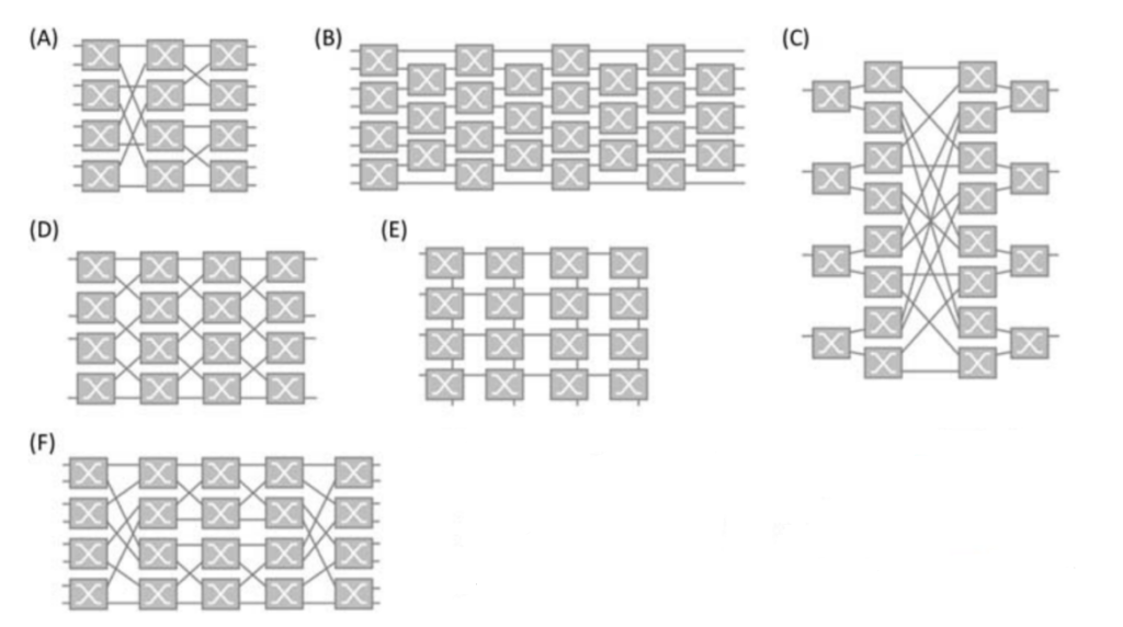
Schematic diagram of several common optical switch topologies
The choice of topology affects key switch characteristics such as blocking behavior, crosstalk, number of components and series.
Integrated optoelectronic switching technology
Currently, several optoelectronic integration platforms are being explored for optical switching.
Silicon-based optoelectronics technology:
- Utilizes mature CMOS manufacturing process
- Large-scale production has cost advantages
- Compact equipment
- High insertion loss and crosstalk
- Usually uses thermo-optical or electro-optical switches
Example: 64×64 Thermo-Optical Benesh switch with 12-18 dB insertion loss
InP Optoelectronics Technology:
- integratable active components (lasers, SOA)
- Low Loss, High Extinction Ratio Switch
- Fast switching speed (nanoseconds)
- Costs more than silicon
Example: Demonstration of lossless operation based on 16×16 SOA
Silicon-based III-V hybrid devices:
- Combine the advantages of InP and silicon
- Enables low-loss switching and integrated gain
- Still an emerging technology
Example: Demonstration of 8×8 switch using flip chip bonding SOA
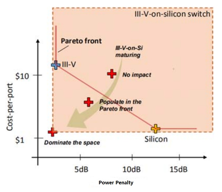
Trade-offs between platforms
Silicon-based optoelectronic switch structure
Silicon-based photonics provides a low-cost platform for large-scale switch integration. Two main types of silicon switches: 1. Thermo-optical (TO) multiplexer switches:
- Using a heater to induce a phase shift
- Relatively slow switching speed (~μs)
- Power consumption is lower than electro-optics
Demonstration data for a 32×32 TO switch using a path-independent loss (PILOSS) architecture is 10.8 dB average insertion loss, 3.5 nm bandwidth, and -20 dB crosstalk.
The larger 64×64 TO Beneš switch achieves 12-18 dB insertion loss and -30 to -44 dB crosstalk over a 45 nm bandwidth.
Electro-Optical (EO) Multiplexer Switch:
- Phase shifting using carrier injection/depletion
- Fast switching (~ns)
- Power consumption is higher than TO
The 32×32 EO Beneš switch has on-chip losses of 13-19 dB, crosstalk of -15 to -25 dB, and switching times of 1-1.2 ns.
InP optical switch structure: InP technology enables monolithic integration of active components such as semiconductor optical amplifiers (SOAs), thereby achieving lossless switching operation.
Key demonstrations include:
- 16×16 Fully Active SOA Switch
- 16×16 active-passive SOA switch for higher power efficiency
- 8x8x8λ spatial and wavelength selective switch
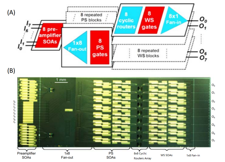
Example of 8x8x8λ InP switch
The switch combines spatial and wavelength domain switching to enable high connectivity and data capacity, achieving >27 dB OSNR, 13.3 dB on-chip loss, and 5 ns reconfiguration time.
Heterogeneous optoelectronic integrated switch structure: Hybrid integration of InP active devices and silicon passive devices combines the advantages of both platforms. Specific methods include:
- Bond InP SOA Flip-chip to silicon-based optoelectronic circuits
- Grow III-V materials on one chip of silicon
- Transfer printing of III-V devices onto silicon
The switch uses silicon AWG for wavelength division multiplexing and flip-chip bonded InP SOA for switching. It achieves 16 dB gain and 34 dB on/off ratio.
Data Center Interconnect Architecture Using Optical Switches
Several architectures that utilize optical switches have been proposed for data center networks: 1. Distributed deep learning training: Optical circuit switches (OCS) are used to dynamically reorganize servers and direct bandwidth to cope with distributed deep learning workloads. A 16-node testbed achieved a 3.6x improvement in network performance compared to a static topology.
Bandwidth control for HPC: The Flexfly architecture uses silicon photonic switches to switch global links between dragonfly groups in HPC networks. This allows for dynamic reconfiguration to match the traffic patterns of the application.
Distributed Data Center: The DACON architecture uses nanosecond optical switches to flexibly configure resources in distributed data centers. Experimental results show that compared with the server-centric architecture, the application runs 1.74 times faster and consumes 34% less power.
Large-scale fast optical circuit switching: Multi-stage Clos networks of silicon-based optical switches can achieve very high port counts. A cascade of 9 stages of 32×32 switches was demonstrated, showing the feasibility of a 131, 072×131, 072-port strictly non-blocking network.
Challenges and Future Prospects
Although optical switches have broad prospects in the data center field, they still face many challenges:
- Packaging: Thermal management, electrical/optical interfaces, and mechanical reliability require further development.
- Scalability: Insertion loss and crosstalk limit the size of the switch. Improvements in design and manufacturing processes are needed.
- Control: A fast, scalable control plane is needed to manage large switch fabrics.
- Power consumption: Reduce static power consumption, especially for devices with a large number of ports.
- Manufacturing process: Strict control of waveguide dimensions is very important for wavelength selective devices.
- Contention resolution: Due to the lack of optical buffers, contention handling becomes difficult.
Future research directions to address these challenges include:
- Advanced packaging technology
- Hybrid/heterogeneous integration of III-V and silicon
- Control algorithm based on machine learning
- New switch architecture that improves scalability
- Integration with emerging computing paradigms (neuromorphic, quantum)
Conclusion
Optical switch fabrics offer solutions to the bandwidth, latency, and energy efficiency challenges of next-generation data center networks. Silicon-based optoelectronics technology provides a path for low-cost, large-scale integration, while III-V materials enable high-performance active devices. Hybrid approaches that combine the advantages of both platforms show great potential.
As manufacturing and integration technologies becoming mature, we can foresee that optical switches will play an increasingly important role in data center architecture. This will advance data-intensive applications such as artificial intelligence and scientific computing while reducing costs and energy consumption. Continued research and development in optical switches is important to meet the interconnect needs of future computing systems.