The Evolution of NVLink, NVSwitch, and NVIDIA H100
The rapid growth of artificial intelligence (AI), high-performance computing (HPC), and data analytics demands cutting-edge interconnect technologies. NVIDIA’s NVIDIA H100 GPU, paired with advanced NVLink and NVSwitch technologies, is at the forefront of this revolution, delivering unparalleled performance for data-intensive workloads. The NVIDIA H100, built on the Hopper architecture, leverages NVLink 4.0 and NVSwitch to enable high-speed, scalable communication between GPUs, transforming data centers and supercomputers. This guide explores the evolution of NVLink and NVSwitch, highlighting how the NVIDIA H100 maximizes their potential for AI, HPC, and enterprise applications. Whether you’re designing an AI supercomputer or upgrading your data center, understanding the synergy of NVIDIA H100, NVLink, and NVSwitch is critical for achieving next-level performance.
The Role of NVIDIA H100 in NVLink and NVSwitch Evolution
The NVIDIA H100 GPU, introduced in 2022 as part of the Hopper architecture, is NVIDIA’s most advanced GPU for AI, HPC, and data analytics. With up to 80 billion transistors and support for FP8 precision, the NVIDIA H100 delivers up to 3x the performance of its predecessor, the A100. Its integration with NVLink 4.0 and NVSwitch is a key milestone in NVIDIA’s interconnect evolution. NVLink 4.0 provides up to 900 GB/s of bidirectional bandwidth, while NVSwitch enables scalable, high-speed communication across multiple NVIDIA H100 GPUs in systems like the NVIDIA DGX H100. This synergy allows the NVIDIA H100 to handle massive AI models, scientific simulations, and real-time analytics with unprecedented efficiency.
2014: Introduction of Pascal Architecture with Tesla P100
In 2014, Nvidia launched the Tesla P100 based on the Pascal architecture. This GPU featured the first-generation NVLink technology, enabling high-speed communication between 4 or 8 GPUs. The NVLink 1.0’s bidirectional interconnect bandwidth was five times that of PCIe 3.0×16. Here’s the calculation:
- PCIe 3.0×16: Bidirectional communication bandwidth of 32GB/s (1GBx16x2).
- NVLink 1.0: Bidirectional interconnect bandwidth of 160GB/s (20GBx4x2).
Due to the absence of NvSwitch chips, the GPUs were interconnected in a mesh topology, where 160GB/s represents the total bandwidth from one GPU to four directly connected GPUs.
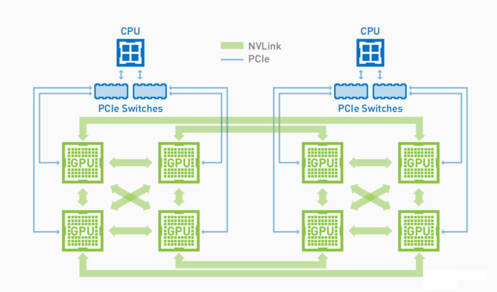
2017: Volta Architecture with V100
In 2017, Nvidia released the Volta architecture with the V100 GPU. The V100’s NVLink increased the per-link unidirectional bandwidth from 20GB/s to 25GB/s and the number of links from 4 to 6, raising the total supported GPU NVLink bandwidth to 300GB/s. However, the V100 DGX-1 system released in 2017 did not feature NvSwitch. The topology was similar to NVLink 1.0, with an increase in the number of links.
2018: Introduction of V100 DGX-2 System
To further enhance inter-GPU communication bandwidth and overall system performance, Nvidia introduced the V100 DGX-2 system in 2018. This was the first system to incorporate the NvSwitch chip, enabling full interconnectivity among 16 SXM V100 GPUs within a single DGX-2 system.
The NVSwitch has 18 NVLink ports, 8 connecting to the GPU and 8 to another NVSwitch chip on a different baseboard. Each baseboard contains six NVSwitches for communication with another baseboard.
2020: Ampere Architecture with A100
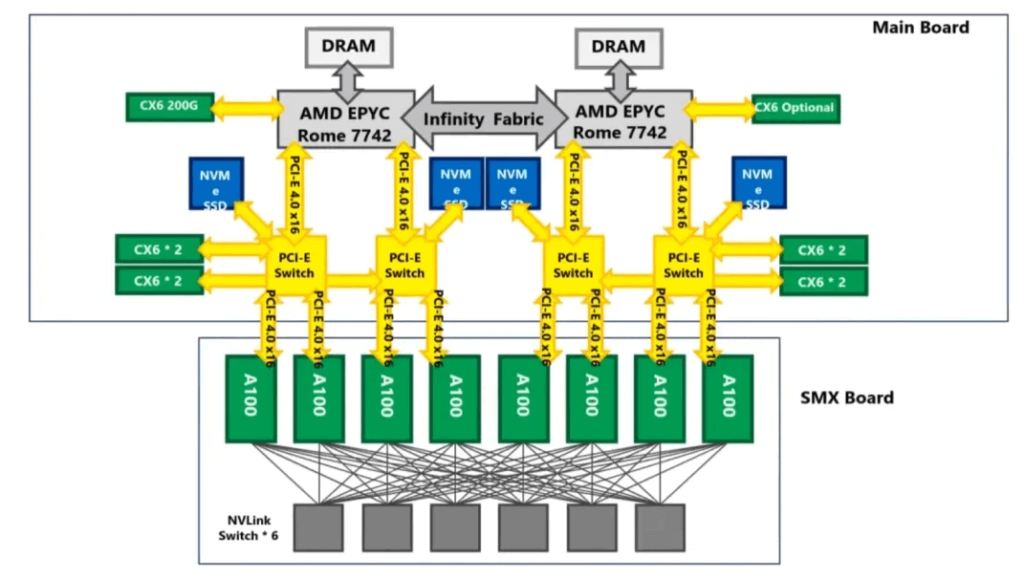
In 2020, Nvidia launched the Ampere architecture with the A100 GPU. The NVLink and NVSwitch chips were upgraded to versions 3.0 and 2.0, respectively. Although the per-link unidirectional bandwidth remained at 25GB/s, the number of links increased to 12, resulting in a total bidirectional interconnect bandwidth of 600GB/s. The DGX A100 system features 6 NVSwitch 2.0 chips, with each A100 GPU interconnected via 12 NVLink connections to the 6 NVSwitch chips, ensuring two links to each NVSwitch.
The logical topology of the GPU system is as follows:
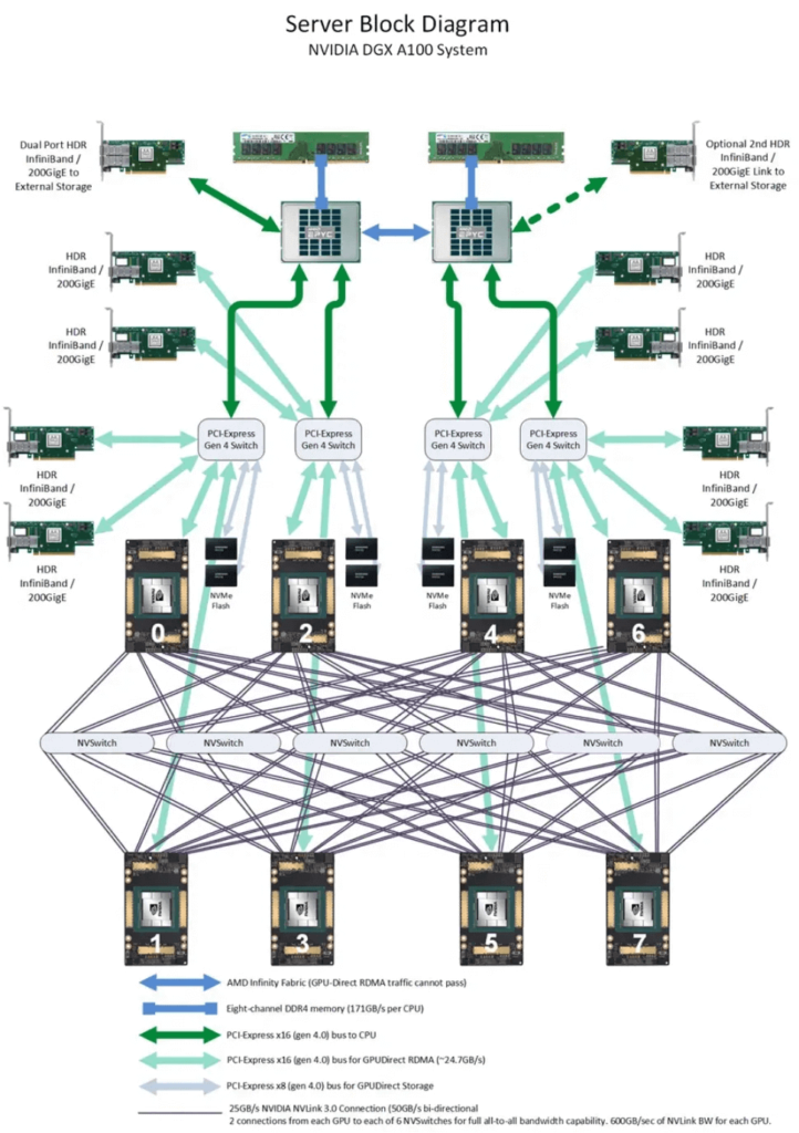
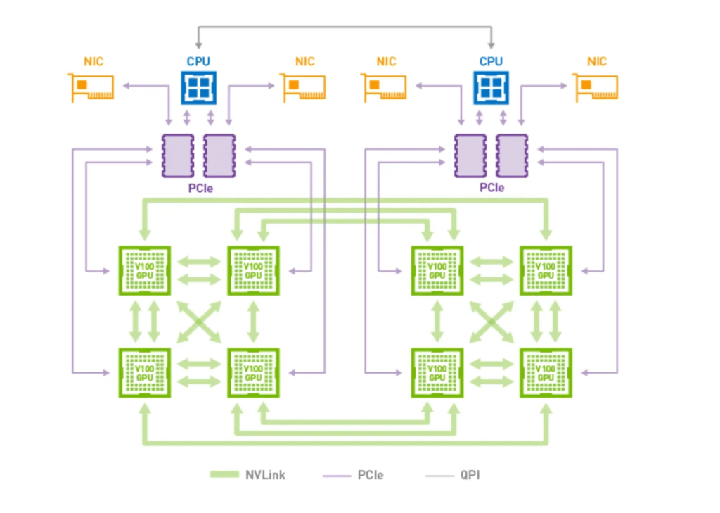
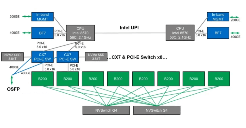
Many people are unclear about the logical relationship between the HGX module and the “server head.” Below is a diagram showing that the SXM GPU baseboard is interconnected with the server motherboard through PCIe links. The PCIe switch (PCIeSw) chip is integrated into the server head motherboard. Both the network card and NVMe U.2 PCIe signals also originate from the PCIeSw.
2022: Hopper Architecture with H100
The H100 GPU, based on the Hopper architecture, was released in 2022 with NVLink and NVSwitch versions 4.0 and 3.0, respectively. While the per-link unidirectional bandwidth remained unchanged at 25GB/s, the number of links increased to 18, resulting in a total bidirectional interconnect bandwidth of 900GB/s. Each GPU is interconnected with 4 NVSwitches using a 5+4+4+5 grouping.
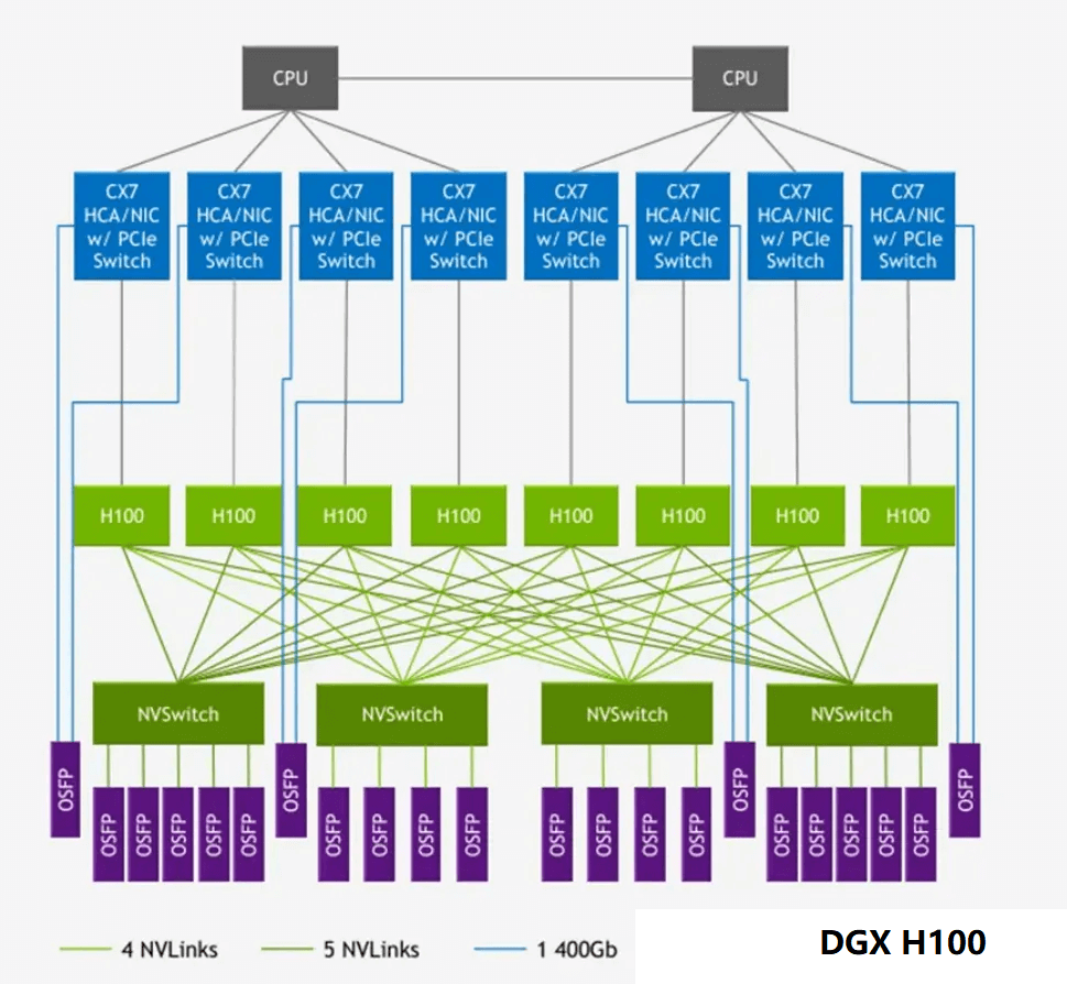
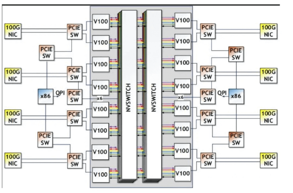
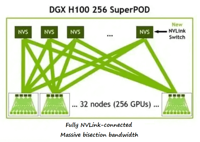
The OSFP interfaces of the NVSwitch chips in the DGX system are used for Nvidia’s larger GPU network, such as in the DGX H100 256 SuperPOD solution.
2024: Blackwell Architecture with B200
In 2024, Nvidia introduced the Blackwell architecture with the B200 GPU, featuring NVLink and NVSwitch versions 5.0 and 4.0, respectively. The per-link unidirectional bandwidth doubled to 50GB/s, with 18 links, resulting in a total bidirectional interconnect bandwidth of 1.8TB/s. Each NVSwitch chip has 72 NVLink 5.0 ports, and each GPU uses 9 NVLink connections to two NVSwitch chips.
With the B200 release, Nvidia also introduced the NVL72, an integrated GPU system that utilizes the NVLink network Switch to achieve full interconnectivity among 72 GPUs.
The logical topology for interconnecting the 72 GPUs using 9 NVLink Switches is as follows:
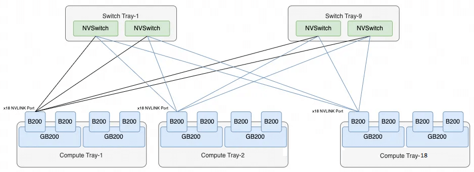
Each B200 GPU has 18 NVLink ports, resulting in a total of 1,296 NVLink connections (72×18). A single Switch Tray contains two NVLink Switch chips, each providing 72 interfaces (144 total). Thus, 9 Switch Trays are required to interconnect the 72 GPUs fully.
Benefits of NVIDIA H100 with NVLink and NVSwitch
The NVIDIA H100 GPU, combined with NVLink 4.0 and NVSwitch, delivers transformative benefits for high-performance computing:
- Unmatched Bandwidth: NVLink 4.0 provides 900 GB/s per NVIDIA H100, enabling rapid data transfers for AI and HPC workloads.
- Massive Scalability: NVSwitch connects up to 256 NVIDIA H100 GPUs, supporting large-scale systems like DGX H100.
- Ultra-Low Latency: Sub-microsecond communication ensures real-time processing for time-sensitive applications.
- AI Optimization: The NVIDIA H100’s Transformer Engine, paired with NVLink, accelerates large language models and generative AI.
- Energy Efficiency: High-bandwidth links reduce the number of connections, lowering power consumption.
- Coherent Memory: NVSHMEM enables cache-coherent memory access across NVIDIA H100 GPUs, boosting efficiency.
- Future-Proofing: Supports emerging workloads like AI inference and scientific simulations.
These benefits make the NVIDIA H100 with NVLink and NVSwitch a cornerstone for next-generation computing.
NVIDIA H100 vs. Other GPUs with NVLink and NVSwitch
Comparing the NVIDIA H100 to other NVLink-enabled GPUs like the A100 helps clarify its advantages:
| Feature | NVIDIA H100 | NVIDIA A100 | NVIDIA V100 |
|---|---|---|---|
| Architecture | Hopper (2022) | Ampere (2020) | Volta (2017) |
| NVLink Version | NVLink 4.0 (900 GB/s) | NVLink 3.0 (600 GB/s) | NVLink 2.0 (300 GB/s) |
| NVSwitch Support | 3rd-Gen (57.6 TB/s) | 2nd-Gen (4.8 TB/s) | 1st-Gen (2.4 TB/s) |
| Performance | 3x A100 (FP8 precision) | 2x V100 | Baseline |
| Memory | 141 GB HBM3 | 80 GB HBM2e | 32 GB HBM2 |
| Use Case | AI, HPC, large-scale analytics | AI, HPC, data analytics | Early AI, HPC |
The NVIDIA H100 with NVLink 4.0 and NVSwitch offers superior performance and scalability, making it the preferred choice for cutting-edge AI and HPC applications.
How to Implement NVIDIA H100 with NVLink and NVSwitch
Deploying the NVIDIA H100 with NVLink and NVSwitch requires careful planning:
- Select Hardware: Use NVIDIA H100 GPUs and NVLink 4.0-compatible systems (e.g., DGX H100, HGX H100).
- Incorporate NVSwitch: Deploy third-gen NVSwitch for multi-GPU scalability in large systems.
- Configure NVLink: Optimize NVLink 4.0 connections for maximum bandwidth (900 GB/s per NVIDIA H100).
- Install Software: Use NVIDIA CUDA, NVSHMEM, and NCCL libraries to enable NVIDIA H100’s cache-coherent features.
- Test Performance: Benchmark data transfers with tools like NCCL to ensure NVIDIA H100 performance.
- Scale Infrastructure: Design for future growth, leveraging NVSwitch to connect multiple NVIDIA H100 GPUs.
Challenges of NVIDIA H100 with NVLink and NVSwitch
While the NVIDIA H100 with NVLink and NVSwitch offers exceptional performance, it has challenges:
- High Cost: NVIDIA H100 GPUs and NVSwitch systems are expensive, requiring significant investment.
- Proprietary Ecosystem: NVIDIA H100 is limited to NVIDIA’s NVLink/NVSwitch, reducing compatibility with non-NVIDIA hardware.
- Configuration Complexity: Optimizing NVIDIA H100 with NVLink 4.0 and NVSHMEM requires expertise.
- Power Consumption: Large-scale NVIDIA H100 deployments with NVSwitch increase power usage.
- Scalability Limits: NVSwitch is optimized for NVIDIA ecosystems, less flexible than open standards like CXL.
Future of NVIDIA H100, NVLink, and NVSwitch
The NVIDIA H100, NVLink, and NVSwitch are set to evolve with emerging technologies:
- Higher Bandwidth: Future NVLink versions may exceed 1 TB/s, enhancing NVIDIA H100 performance.
- AI Optimization: Advanced NVSHMEM and NVSwitch will streamline next-gen AI models on NVIDIA H100.
- Broader Integration: NVIDIA H100 may support hybrid interconnects like CXL for heterogeneous systems.
- Energy Efficiency: Future designs will reduce power consumption for NVIDIA H100 deployments.
- Edge AI: NVIDIA H100 with NVLink will support low-latency AI inference at the edge.
Related Products:
-
 NVIDIA MMA4Z00-NS400 Compatible 400G OSFP SR4 Flat Top PAM4 850nm 30m on OM3/50m on OM4 MTP/MPO-12 Multimode FEC Optical Transceiver Module
$550.00
NVIDIA MMA4Z00-NS400 Compatible 400G OSFP SR4 Flat Top PAM4 850nm 30m on OM3/50m on OM4 MTP/MPO-12 Multimode FEC Optical Transceiver Module
$550.00
-
NVIDIA MMA4Z00-NS-FLT Compatible 800Gb/s Twin-port OSFP 2x400G SR8 PAM4 850nm 100m DOM Dual MPO-12 MMF Optical Transceiver Module
$650.00
-
NVIDIA MMA4Z00-NS Compatible 800Gb/s Twin-port OSFP 2x400G SR8 PAM4 850nm 100m DOM Dual MPO-12 MMF Optical Transceiver Module
$650.00
-
NVIDIA MMS4X00-NM Compatible 800Gb/s Twin-port OSFP 2x400G PAM4 1310nm 500m DOM Dual MTP/MPO-12 SMF Optical Transceiver Module
$900.00
-
NVIDIA MMS4X00-NM-FLT Compatible 800G Twin-port OSFP 2x400G Flat Top PAM4 1310nm 500m DOM Dual MTP/MPO-12 SMF Optical Transceiver Module
$1199.00
-
NVIDIA MMS4X00-NS400 Compatible 400G OSFP DR4 Flat Top PAM4 1310nm MTP/MPO-12 500m SMF FEC Optical Transceiver Module
$700.00
-
NVIDIA(Mellanox) MMA1T00-HS Compatible 200G Infiniband HDR QSFP56 SR4 850nm 100m MPO-12 APC OM3/OM4 FEC PAM4 Optical Transceiver Module
$139.00
-
NVIDIA MFP7E10-N010 Compatible 10m (33ft) 8 Fibers Low Insertion Loss Female to Female MPO Trunk Cable Polarity B APC to APC LSZH Multimode OM3 50/125
$47.00
-
NVIDIA MCP7Y00-N003-FLT Compatible 3m (10ft) 800G Twin-port OSFP to 2x400G Flat Top OSFP InfiniBand NDR Breakout DAC
$260.00
-
NVIDIA MCP7Y70-H002 Compatible 2m (7ft) 400G Twin-port 2x200G OSFP to 4x100G QSFP56 Passive Breakout Direct Attach Copper Cable
$155.00
-
NVIDIA MCA4J80-N003-FTF Compatible 3m (10ft) 800G Twin-port 2x400G OSFP to 2x400G OSFP InfiniBand NDR Active Copper Cable, Flat top on one end and Finned top on other
$600.00
-
NVIDIA MCP7Y10-N002 Compatible 2m (7ft) 800G InfiniBand NDR Twin-port OSFP to 2x400G QSFP112 Breakout DAC
$190.00