NVIDIA released Blackwell B200 in March of this year, which is known as the world’s most powerful AI chip. How is it different from the previous A100, A800, H100, and H800?
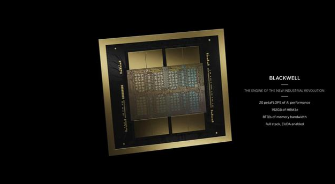
Blackwell B200
NVIDIA GPU Architecture Evolution
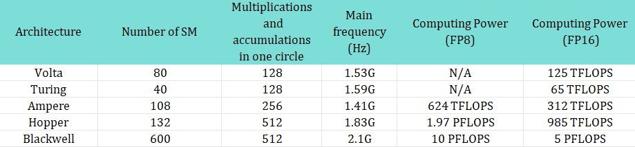
Let’s first review the computing power development history of NVIDIA AI accelerator cards:
The first generation of AI accelerator cards is called Volta, which is NVIDIA’s first tensor core architecture designed specifically for AI computing.
The second-generation tensor computing architecture is called Turing, which represents the graphics card T4.
The third-generation tensor computing architecture Ampere has finally come to the A100 series graphics cards that we are more familiar with.
With the support of chip process upgrades, the SM of a single card has doubled to 108. The number of cores in the SM is the same as that of V100, but through the upgrade of the computing unit circuit, the core can complete 256 floating-point multiplications and accumulations in each cycle, which is twice that of the old architecture. The 8-bit floating-point (FP8) computing mode was added to better meet the needs of deep learning at the time. One 16-bit floating-point core can be calculated as two 8-bit floating-point cores, doubling the computing power. The main frequency has dropped slightly to 1.41GHz. Therefore, in the end, the computing power of the A100 graphics card reached nearly 5 times that of the V100, which is 108*8*256*1.41GHz*2 =624 TFLOPS (FP8).
Ampere Architecture
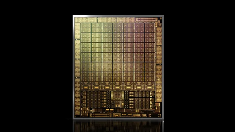
The fourth-generation architecture Hopper is the H100 series graphics card that NVIDIA just released last year, has been adopted by OpenAI for large language model training, and has been banned due to computing power issues.
The number of SMs (132) of this graphics card has not increased significantly compared to the previous generation, but because of the new Tensor Core architecture and asynchronous memory design, the number of FP16 multiplications and accumulations that can be completed by a single SM core in one cycle has doubled to 512 times. The main frequency was slightly increased to 1.83GHz, and the computing power of a single card finally reached an astonishing 1978 Tera FLOPS (FP8), which was the first time it entered the PFLOPS (1.97 Peta FLOPS) field.
Hopper Architecture
What kind of progress has the fifth-generation architecture Blackwell made on this computing power ladder? According to public data, if the new FP4 data unit is adopted, GB200 will be able to achieve 20 Peta FLOPS computing power in reasoning tasks. If it is restored back to FP8, it should also have an amazing 10 PFLOPS, which is about 5 times the improvement over H100.
Public data shows that the main frequency of Blackwell’s processor is 2.1GHz. Assuming the architecture is not significantly updated, Blackwell will have 600 SMs, nearly four times that of H100. Blackwell has two dies, so the number of SMs in a single-die graphics card is twice that of H100.
It can be concluded that with each generation of architecture upgrading, the computing power of a single GPU has increased several times. Here, we list the computing power progress chart from the Volta architecture to the present for your reference:
Computing power progress chart
A100 vs A800, H100 vs H800
Why do we need A800 when we have A100? Let’s first talk about the background.
In October 2022, the United States introduced new regulations to restrict semiconductor exports to China, including export restrictions on high-performance computing chips to China’s mainland. Performance metrics of NVIDIA’s A100 chip are used as the limiting standard, that is, high-performance computing chips that meet both of the following conditions are regulated:
(1) The chip’s I/O bandwidth transmission rate is greater than or equal to 600 G byte/s;
(2) The sum of the bit length of each operation of the “digital processing unit, raw computing unit” multiplied by the computing power calculated by TOPS is greater than or equal to 4800TOPS.
The conditions make it impossible to export NVIDIA A100/H100 series and AMD MI200/300 series AI chips to China.
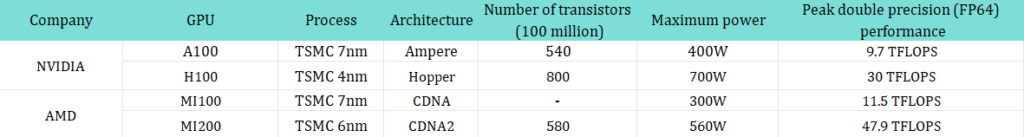
Comparison of Nvidia and AMD GPUs
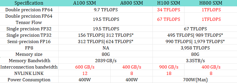
In order to comply with US restrictions while meeting the needs of Chinese customers, NVIDIA launched the A800, a replacement for the A100. Judging from the official parameters, A800 mainly reduces the transmission rate of NVLink from 600GB/s of A100 to 400GB/s, with other parameters basically the same as A100.
In 2023, NVIDIA released the new generation H100 GPU based on 4nm process, with 80 billion transistors and 18,432 cores. Similarly, NVIDIA has also launched a special version of H800 for the Chinese market.
Chip comparison
In fact, A800 has made adjustments to the interconnection bandwidth, namely the N-dimensional chain and link part, down from 600G/s of A100 to 400G/s. However, in other aspects, such as double-precision, single-precision, and semi-precision, there is no change in AI computing power.
Relatively speaking, H800 has made major adjustments. It not only made adjustments in terms of links, maintaining 8 NVlinks and 400G bidirectional interconnection bandwidth, but also reduced the double-precision computing to zero. This is critical for the HPC field because the double-precision computing power of FP64 is directly reduced to one, which means that you can hardly use it.
Next, let’s take a look at which businesses will be greatly affected by the adjustments.
Large model battlefield: After A800 was adjusted, the efficiency of large model training was reduced. A800 SXMM mainly reduced the data transmission efficiency between GPU cards and the bandwidth was reduced by 33%. Taking GPT-3 as an example, its scale reaches 175 billion, and it requires multiple GPUs for combined training. If the bandwidth is insufficient, the performance will drop by about 40%. Considering the cost-effectiveness of A 800 and H 800, Chinese users still prefer A 800. Since the adjusted A800 and H800 have decreased training efficiency, and they need to exchange some data during the training process between cards, their reduced transmission rate leads to a decrease in their efficiency.
HPC: A800 and A100 have the same dual-precision computing power, so they are not impacted in the field of high-performance scientific computing. However, the annoying thing is that H800 directly reduces the dual-precision computing power to 1 TFLOPS, so it is not allowed to be used. This has a huge impact on the super computing field.
Therefore, the impact is obvious. In the fields of AIGC and HPC, some Chinese companies may be left behind by foreign companies. This is foreseeable, so in some cases, if we want computing power to achieve a certain performance, the investment may be higher. In addition, we can only borrow a shell company from abroad and set up a branch to place the task of large model training abroad. We only need to use the training results in China. However, this is only a temporary solution, especially when facing the risk of data leaving the country.
Summary
As we all know, the United States is imposing increasingly strict restrictions on Chinese chips, including GPUs. In 2022, the United States banned high-performance GPU chips, including A100, H100, etc., and in 2023 it banned A800, H800, L40, L40S, and even the desktop graphics card RTX 4090.
Therefore, Chinese technology companies are also actively adjusting their industrial strategies to prepare for reducing the use of Nvidia chips in the future, thereby avoiding the huge cost of constantly adjusting technology to adapt to new chips. Cloud vendors such as Alibaba and Tencent have shifted some advanced semiconductor orders to local companies such as Huawei and relied more on their internally developed chips. Companies such as Baidu and ByteDance have also taken similar measures. Obviously, Chinese companies have chosen to explore the way forward through a three-pronged approach of ” NVIDIA + self-developed + domestic chips “.
Related Products:
-
 NVIDIA MMA4Z00-NS400 Compatible 400G OSFP SR4 Flat Top PAM4 850nm 30m on OM3/50m on OM4 MTP/MPO-12 Multimode FEC Optical Transceiver Module
$550.00
NVIDIA MMA4Z00-NS400 Compatible 400G OSFP SR4 Flat Top PAM4 850nm 30m on OM3/50m on OM4 MTP/MPO-12 Multimode FEC Optical Transceiver Module
$550.00
-
NVIDIA MMA4Z00-NS-FLT Compatible 800Gb/s Twin-port OSFP 2x400G SR8 PAM4 850nm 100m DOM Dual MPO-12 MMF Optical Transceiver Module
$650.00
-
NVIDIA MMA4Z00-NS Compatible 800Gb/s Twin-port OSFP 2x400G SR8 PAM4 850nm 100m DOM Dual MPO-12 MMF Optical Transceiver Module
$650.00
-
NVIDIA MMS4X00-NM Compatible 800Gb/s Twin-port OSFP 2x400G PAM4 1310nm 500m DOM Dual MTP/MPO-12 SMF Optical Transceiver Module
$900.00
-
NVIDIA MMS4X00-NM-FLT Compatible 800G Twin-port OSFP 2x400G Flat Top PAM4 1310nm 500m DOM Dual MTP/MPO-12 SMF Optical Transceiver Module
$1199.00
-
NVIDIA MMS4X00-NS400 Compatible 400G OSFP DR4 Flat Top PAM4 1310nm MTP/MPO-12 500m SMF FEC Optical Transceiver Module
$700.00
-
NVIDIA(Mellanox) MMA1T00-HS Compatible 200G Infiniband HDR QSFP56 SR4 850nm 100m MPO-12 APC OM3/OM4 FEC PAM4 Optical Transceiver Module
$139.00
-
NVIDIA MFP7E10-N010 Compatible 10m (33ft) 8 Fibers Low Insertion Loss Female to Female MPO Trunk Cable Polarity B APC to APC LSZH Multimode OM3 50/125
$47.00
-
NVIDIA MCP7Y00-N003-FLT Compatible 3m (10ft) 800G Twin-port OSFP to 2x400G Flat Top OSFP InfiniBand NDR Breakout DAC
$260.00
-
NVIDIA MCP7Y70-H002 Compatible 2m (7ft) 400G Twin-port 2x200G OSFP to 4x100G QSFP56 Passive Breakout Direct Attach Copper Cable
$155.00
-
NVIDIA MCA4J80-N003-FTF Compatible 3m (10ft) 800G Twin-port 2x400G OSFP to 2x400G OSFP InfiniBand NDR Active Copper Cable, Flat top on one end and Finned top on other
$600.00
-
NVIDIA MCP7Y10-N002 Compatible 2m (7ft) 800G InfiniBand NDR Twin-port OSFP to 2x400G QSFP112 Breakout DAC
$190.00