The NVIDIA A100 GPU has transformed high-performance computing (HPC) and artificial intelligence (AI). This cutting-edge design for complex computational tasks in any industry provides unparalleled performance, scalability, and flexibility. In terms of architecture, capabilities, and applications, this blog will give an in-depth analysis of it. The A100 establishes a new standard for computational efficiency and power, which can be used to speed up deep learning models or improve scientific research. This post is for you if you work with data as a data scientist or AI researcher; also, if your company needs more AI and HPC capabilities, then the article might be helpful too – we’ll be discussing how NVIDIA A100 meets or exceeds your computation requirements.
Table of Contents
ToggleWhat is the NVIDIA A100 GPU?
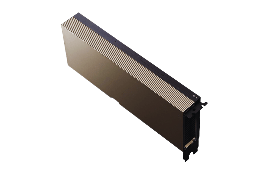
Overview of the NVIDIA A100 GPU
Designed specifically to handle the hardest of artificial intelligence and HPC loads, the NVIDIA A100 GPU is the most recent in a series of NVIDIA data center GPUs. It gives up to 20 times higher performance than its predecessors by using Ampere architecture that breaks new ground. The A100 comes with third-generation Tensor Cores which allow for deep learning as well as matrix calculations where both dense and sparse operations are involved in processing rapidly and effectively. This also supports structural sparsity while enabling multi-instance GPU (MIG) for workload isolation optimization so that resources can be used optimally based on need. With such ability, it can be used either for training massive neural networks or accelerating enterprise-level data analytics – making it a versatile, powerful part of any modern computational setup.
Key Specifications of the A100 GPU
The NVIDIA A100 GPU has a strong feature set that can handle the most difficult computational workloads.
- Architecture: Ampere.
- CUDA cores: 6,912.
- Third-generation Tensor Cores: 432 Tensor Cores.
- Memory: 40GB or 80GB High Bandwidth Memory (HBM2e).
- Memory Bandwidth: up to 1,555 GB/s.
- Peak FP64 Performance: up to 9.7 teraflops.
- Peak FP32 Performance: up to 19.5 teraflops.
- Peak FP16 Performance with Sparsity: up to 312 teraflops.
- MIG Capability: Supports up to seven independent GPU instances.
- Interconnect: NVLink (600 GB/s bidirectional) and PCIe Gen4 support.
These specs show that the A100 performs incredibly well in Artificial Intelligence as well as High-Performance Computing (HPC) applications. With large numbers of CUDA cores and Tensor Cores combined with high memory bandwidth and capacity, it is able to effectively manage huge datasets and complex computations. Moreover, MIG allows many different workloads to run on one GPU at the same time, which optimizes resource utilization, thus increasing overall throughput.
Comparison with Previous NVIDIA GPUs
The NVIDIA A100 GPU is much better than the past versions, such as the V100 and P100. One of the main advancements is the switch from Volta architecture, which was used in V100, to Ampere architecture in A100, which comes with more CUDA cores, translating to 6912 (versus 5120 in V100) and introducing third-generation Tensor Cores, thereby boosting AI and computational performance. In addition, memory capacity has been increased by a significant factor while also increasing its bandwidth; this means that up to 80GB HBM2e can be supported with 1555GB/s bandwidth when compared against maximums of 32GB HBM2 & 900GB/s for v100, respectively. Besides being able to support seven different single GPU instances concurrently thanks to Multi-Instance GPUs (MIG), A 100 allows for an even more flexible allocation of resources, thus making it efficient. These improvements together make sure that a variety of demanding tasks in AI or HPC are done faster on A100 than any other model before it, showing how NVIDIA keeps striving for perfection through continuous innovation.
How Does the NVIDIA A100 GPU Enhance AI and Data Analytics?
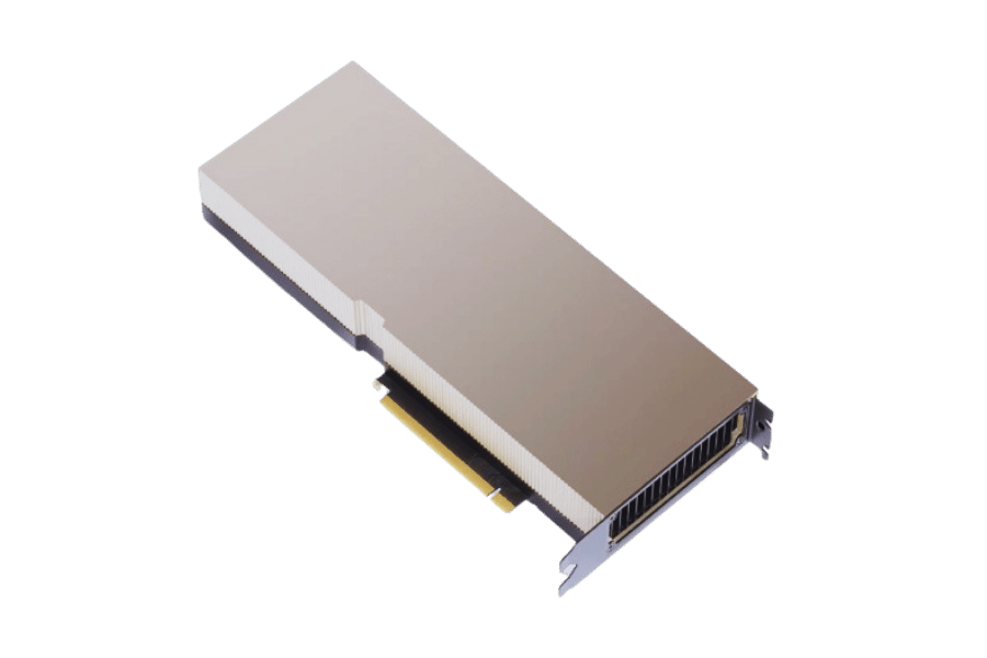
AI Capabilities of the NVIDIA A100
The NVIDIA A100 GPU takes AI and data analytics to new heights with a number of key features. First, this device has third-generation Tensor Cores, which can multiply the speed of AI training and inference by up to 20 times over previous models. Second, the memory capacity is huge — up to 80GB HBM2e — so datasets can be bigger and models more complex than ever before for advanced AI applications. Third, one GPU can handle several parallel AI tasks simultaneously thanks to Multi-Instance GPU (MIG) technology onboard; this saves resources and speeds things up by cutting down on latency. Fourth, mixed-precision computing is supported by the A100: it makes fast but accurate calculations possible when needed most during artificial intelligence workloads where both qualities matter most. In this single sentence alone, these capabilities allow unmatched swiftness and efficiency throughout numerous types of machine learning projects dealing with information analysis that were unimaginable before now.
Benefits of Data Analytics
The NVIDIA A100 GPU offers significant enhancements for data analytics through its advanced architecture and features. First of all, its high memory bandwidth is good for working with large data sets by processing them faster and reducing the time of data transfer. The Multi-Instance GPU (MIG) in A100 enables it to be partitioned into seven separate machines, each capable of handling different analytics tasks at the same time, thus maximizing the efficiency with which resources are used depending on workload requirements. In addition, this device has hardware support for accelerated transformation as well as filtering operations applied to information before it gets analyzed.
What is more, mixed-precision computing and tensor operations are supported by A100, which speeds up calculations required for real-time analysis. Another thing worth mentioning is that it can seamlessly integrate with popular big data frameworks like Apache Spark or RAPIDS, so users don’t need to make any changes in their existing pipelines while still being able to take advantage of its computational power. It’s evident from these indicators that A100 can greatly increase the speed, scalability, and efficiency of working with large amounts of data during analytic processes.
Applications in Real-World Scenarios
In various sectors, the NVIDIA A100 GPU is applicable in real-world situations. In medical care, this element quickens processing of medical imaging data thus speeding up diagnosis through its enhanced computational power. It can process MRI or CT scans for example on the spot thereby improving efficiency and precision in health appraisals.
Financial services it is used to manage risks quickly by processing huge datasets with ease alongside fraud detection and instant trading analytics. This means that its speed (throughput) and time delay (latency) are both low, which are essential for running complicated algorithms meant to examine market trends as well as predictive insights.
The scientific research area utilizes the high-performance computing capabilities of A100, especially in tasks like molecular dynamics simulations and weather forecasting, among others related to this field. The mixed-precision computing of the GPU improves these simulations, making them more accurate, hence leading to timely discoveries.
Artificial intelligence (AI) together with machine learning (ML) heavily relies on large-scale neural networks when training models using A100 GPU so as to greatly reduce on training durations. This is important for creating advanced AI models applied in such areas as natural language processing; autonomous driving among many others within robotics field.
To sum it up, the flexibility plus great performance shown by NVIDIA A100 GPU makes it an indispensable tool across different disciplines, thereby enhancing the innovation and effectiveness of numerous applicable ideas.
What Makes the A100 GPU Ideal for Servers?
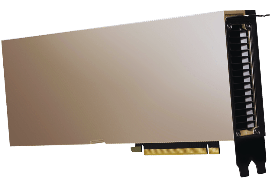
Scalability and Efficiency
Server environments can benefit greatly from the NVIDIA A100 GPU due to its scalability and efficiency. Through the use of multi-instance GPU (MIG) technology, one can partition a single A100 into as many as seven smaller isolated instances that allow several workloads at once without competing for resources. Thus, resource utilization is optimized while performance is maximized, which suits well data centers dealing with various heavy computational tasks. Moreover, no other system can match it when it comes to power saving thanks to high-memory bandwidths and tensor cores, which give best-in-class performance per watt, therefore reducing energy consumption without compromising on speed. The unique blend of these features makes sure that A100 is capable of meeting any modern server app requirement, be it AI training or scientific calculations, etcetera.
Power Management and Consumption
The NVIDIA A100 GPU has sophisticated power management technology, which saves energy while maximizing performance. Its key indicators of performance include a maximum power draw of 400 watts under full load. But for high-performance tensor cores and efficient architecture, still the performance per watt remains very high even with such power consumption.
The A100, in server applications, uses dynamic power scaling that alters the amount of electricity used according to task requirement. This ensures not only good performance during low intensity or idle operations but also allows the GPU to scale up well when there is high demand for it.
Moreover, this adaptive power shading by NVIDIA on A100 allocates more electricity to essential areas whenever necessary while reducing it elsewhere that needs less power. Such intelligent sharing helps in balancing between performance and energy efficiency.
In brief terms; among others are these features of A100’s power management:
- Maximum Power Consumption: 400 watts.
- Performance per Watt: Optimized by tensor cores and architecture.
- Dynamic Power Scaling: Adjusts based on workload demands.
- Adaptive Power Shading: Intelligent power distribution for efficiency.
Therefore, these characteristics enable the NVIDIA A100 GPU to be highly efficient in modern server environments where intensive applications need support without compromising energy usage control.
How Does the NVIDIA A100 Tensor Core GPU Improve Performance?
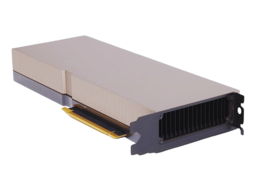
Introduction to Tensor Core Technology
The A100 GPU’s performance improvements are all because of NVIDIA’s Tensor Core technology. Units for processing, specialized for deep learning, are what tensor cores are about. These types of cores make possible the execution of mixed-precision matrix operations that train and infer neural networks among other things. In comparison to standard GPU cores, which do dense matrix multiplications, tensor cores perform this task at much faster rates, thus increasing computational workloads’ speed while reducing complex algorithm processing time. As a result, throughputs increase significantly, and so do efficiencies, therefore making it extremely suitable for natural language processing systems or any other application involving heavy-duty deep learning like image recognition software used in scientific research – the A100 GPU.
Performance Metrics and Benchmarks
Different metrics and benchmarks can be used to assess the performance of the NVIDIA A100 Tensor Core GPU. These measurements indicate how well the device handles high-performance computing tasks, especially those related to deep learning. Several key performance metrics include:
FP64 Performance: Up to 9.7 teraflops are delivered by this device which is used for scientific computing and simulations.
FP32 Performance: Traditional single-precision workloads require up to 19.5 teraflops.
Tensor Float 32 (TF32) Performance: For deep learning training without loss of precision, up to 156 teraflops have been optimized.
INT8 Performance: Machine learning applications need inference tasks that perform up to 624 TOPs (Tera Operations per Second).
Moreover, there are also some benchmarks that point out how great the A100 performs:
MLPerf Benchmarks:
- The A100 surpassed prior-generation GPUs by a wide margin in MLPerf benchmarks for image classification, object detection, and natural language processing tasks.
Deep Learning Training Benchmarks:
- Compared with previous GPU models, the A100 cuts training times in popular deep learning frameworks like TensorFlow and PyTorch by as much as 20x.
High-Performance Computing (HPC) Benchmarks:
- The LINPACK benchmark in HPC applications demonstrates excellent performance of double-precision floating-point capabilities necessary for scientific and engineering computations by the A100.
These taxing benchmarks and metrics verify the technically advanced parameters of the A100 GPU and show its ability to deliver outstanding performance across different computational environments that demand it.
Third-Generation Tensor Cores Explained
Third generation tensor cores are designed for ultra-low efficiency in AI and HPC operations. These cores support many types of data that include TF32 which ensures numerical stability and accuracy while delivering up to 20 times more performance than FP32 operations. This development is invaluable for deep learning training as it enables quicker calculations without manual management of mixed precision requirements.
Furthermore, these third-generation Tensor Cores have the ability to recognize and use the most important parts of a computation through structural sparsity doubling their throughput. This characteristic employs sparsity patterns to enhance efficiency in neural network models. Additionally, they can work with various data formats such as FP16, bfloat16, INT8 or INT4 thus ensuring that all workloads perform optimally.
To sum it up, Third Generation Tensor Cores expand computational power by extending precision coverage, streamlining data handling, and widening input channels so that throughput is maximized towards modern artificial intelligence systems and high-performance computing applications alike.
What are the Features of the NVIDIA A100 PCIe Version?
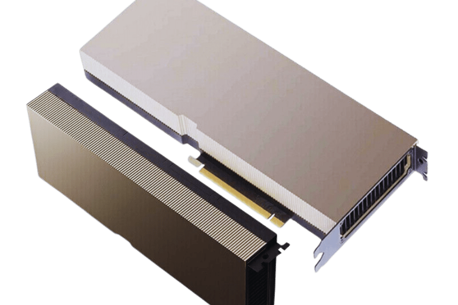
Differences Between PCIe and SXM Versions
To meet different performance and integration requirements, the NVIDIA A100 GPU is available in PCIe and SXM forms. The PCIe version of the card was built to fit with typical server architectures which makes it compatible with a wide range of systems as it can be deployed easily on them. Additionally, this model has less power consumption than its counterparts and can therefore be used more widely across current server infrastructures.
On the other hand, NVidia’s DGX systems use the SXM variant, which supports higher power budgets and better thermal management. This allows for higher performance thresholds as well as greater computational density that is required by highly demanding AI and HPC workloads. Also, unlike PCIe, NVLink interconnects are found on SXM cards; hence, they have faster interconnect speeds between GPUs, thus enabling more efficient multi-GPU configurations.
In conclusion: The A100 GPU in PCIe form offers wider compatibility while being easy to deploy but lacks performance compared to its SXM counterpart which delivers higher performance levels along with better interconnections that suit intense computational tasks best.
PCIe Advantages in Different Use Cases
In several different applications the NVIDIA A100 PCIe edition has a lot of benefits because of its design and compatibility features. Below are some advantages as well as relevant technical parameters:
Compatibility with Standard Server Architectures
- PCIe version can be integrated with various existing server systems thereby eliminating the need for specialized hardware.
- Technical Parameter: Uses PCI Express 4.0 interface which ensures compatibility and high data transfer rates of up to 16 GT/s per lane.
Ease of Deployment
- It is easy to install in standard server environments which contributes towards faster deployment times and reduced complexity of system integration.
- Technical Parameter: Supports standard PCIe slots hence making scalability easy and allowing for quick upgrade paths.
Lower Power Consumption
- Compared to SXM version, this version consumes less power thus can work best in energy-sensitive areas.
- Technical Parameter: The power consumption is about 250 Watts while that of SXM version is 400 Watts.
Accessibility for a Broader Range of Users
- The PCIe edition is compatible and user-friendly therefore it can be used by many people ranging from small businesses to large data centers.
- Technical Parameter: It allows the use commodity server hardware where you utilize already made investments but still get strong computational powers.
Looking at these technical parameters makes it clear that the NVIDIA A100 PCIe edition addresses different deployment scenarios by balancing performance, power consumption and ease of integration.
How Can the NVIDIA A100 GPU Optimize Server Setups?

Multi-Instance GPU (MIG) Technology
The NVIDIA A100 GPU permits the division of its resources into separate units that act as individual GPUs through Multi-Instance GPU (MIG) technology. With this feature, one A100 GPU can cater to many different applications and users at the same time, thereby maximizing resource utilization efficiency. More importantly, these instances are flexible enough to be assigned on-demand while ensuring interference-free allocation of necessary GPU resources for each workload. Businesses can optimize their server configurations by matching specific task requirements with appropriate levels of graphical processing performance using MIG technology, thus enabling them to utilize maximum computing capacity while minimizing delays caused by network traffic or data transfers.
Efficiency in High-Performance Computing (HPC)
Advanced architectural features and technologies make the NVIDIA A100 GPU efficient in high-performance computing (HPC) settings. One of its advantages is that it reduces power consumption while maintaining computational performance. This equilibrium is attained through various technical improvements:
Mixed-Precision Computing with Tensor Cores:
- Technical Parameter: The A100 GPU has third-generation Tensor Cores, which support FP16, BFLOAT16, TF32, FP64, and INT8 precisions.
- Justification: These Tensor Cores increase throughput and decrease power needs by adjusting processing precision dynamically based on the job.
High Memory Bandwidth:
- Technical Parameter: Up to 1.6 TB/sec memory bandwidth is provided by the A100 GPU.
- Justification: This enables faster transfer rates for data and better handling of large datasets – a key requirement in HPC workloads efficiency improvement.
Scalable Performance with NVLink:
- Technical Parameter: NVLink interconnects used by the A100 provide much higher data bandwidth between GPUs than PCIe does.
- Justification: NVLink makes scaling multiple GPUs easier, thus increasing compute power without creating data traffic jams that would be brought about by higher levels of power usage per wattage consumed.
Multi-Instance GPU (MIG) Technology:
- Technical Parameter: Each A100 can have up to seven MIG-based GPU instances.
- Justification: With such technology, it’s possible to optimize the usage of resources so that different types of tasks can use one card, thus reducing idle time while increasing efficiency at the same time for various HPC jobs.
Dynamic Resource Management:
- Technical Parameter: Reallocation support for dynamic reassignment among different applications running concurrently on the same physical device.
- Justification: Allocation of adaptive cores according to demand application being run at any particular moment helps prevent wastage or underutilization thereby saving energy spent on powering them continuously up and down again each time the need arises from within an environment where many such devices are found together, sharing common infrastructure.
The NVIDIA A100 GPU can therefore be said to deliver optimized performance for HPC environments by integrating these technical parameters which result in higher efficiency, reduced power consumption and effective scaling of computational tasks.
Integration with the NVIDIA Data Center Platform
When integrating the NVIDIA A100 GPU with the NVIDIA Data Center Platform, a range of tools and technologies are brought in that maximize the capabilities of the GPU for high-performance computing (HPC). The platform includes NVIDIA GPU Cloud (NGC), which provides a complete catalog of pre-trained models, industry-specific SDKs, and optimized frameworks for streamlining AI development and deployment. It is important to note that the NVIDIA NGC software stack ensures smooth compatibility as well as top performance by giving containerized environments, which makes deployment of HPC workloads across different clouds or on-premises systems easy.
Moreover, developers who want their applications to run faster on an A100 GPU need NVIDIA’s CUDA toolkit because it comes with necessary libraries, tools, and technologies that accelerate computation tasks effectively on these devices. Additionally, cuDNN and TensorRT, among other deep learning libraries from Nvidia, enhance speed and accuracy during complex neural network training and inferencing tasks by this hardware-accelerated computing unit.
Additionally, there are some management tools supported by the platform like a robustness monitoring tool called NVIDIA GPU Operator or a scaling resource toolset known as NVIDIA Data Center Workload Manager (DCGM); these enable efficient monitoring; maintenance, scaling up/down, etc., so as to have the best performance out of available resources while keeping alive system functionality where necessary.. In addition, this security consciousness sees integration into the solution’s advanced data protection capabilities, thus making it a one-stop-shop package for any modern data center interested in utilizing the power provided by NVidia A100 GPUs.
Frequently Asked Questions (FAQs)
Q: Why does the NVIDIA A100 suit high-performance computing and AI workloads?
A: The NVIDIA A100 is designed for resource-intensive tasks in areas such as AI and high-performance computing with up to 20 times more power than the previous NVIDIA Volta generation. It constitutes an essential part of the entire data center solution by NVIDIA which demonstrates unmatched performance across different applications.
Q: How can a graphics card support AI models like A100?
A: To be precise, the A100 graphics card is fine-tuned for AI models; therefore, it provides higher speed at 20x than any other GPU that enables workload scaling capability. This is powered by its advanced tensor cores – the highest-performing graphics processor for end-to-end AI and HPC jobs in the world.
Q: What do you understand by tensor cores in the A100?
A: When it comes to optimized machine learning models, no other GPU on earth beats A100 tensor core GPUs because they offer better performance plus faster processing of complex computations required for HPCs & AIS.
Q: Can I use one A100 for multiple tasks?
A: Yes, an A100 can be partitioned into seven isolated GPU instances, thus allowing concurrent running of several tasks and enhancing efficiency while managing multi-tasking workloads.
Q: How does it compare against prior NVidia Volta generations?
A: With 20 times more computation power than previous Nvidia volta generations, a single unit of measurement may perform higher functions and process advanced workloads much quicker too thanks to this feature alone – provided by those wonderful little things called tensor core chips contained inside every one these new age graphic cards known collectively as ‘NVIDIA GeForce RTX 30 Series‘.
Q: What are some key features offered by a variant having 80GB capacity?
A:The larger memory capacity (80GB) available in this particular model ensures that huge amounts of data can be processed without any issues arising – making it perfect for use with large datasets or complex models commonly found in AI or HPC environments.
Q: Why is A100 important to NVIDIA’s data center solution?
A: The A100 represents the engine of NVIDIA’s complete data center platform which enables the world’s most powerful compute environments optimized for AI, HPC & enterprise applications.
Q: How does this GPU scale workload effectively?
A: By allowing users to partition it into seven isolated instances of itself, thereby enabling them to run multiple tasks simultaneously so that they can better manage diverse and concurrent workloads effectively.
Q: What types of platforms benefit most from using an A100 GPU?
A: Data centers that specialize in AI and high-performance computing (HPC); however, any platform requiring massive amounts of computational power would also greatly benefit from having these types of graphics cards installed within their system cabinets.
Q: How does it compare with other Tensor Core GPUs available on the market today?
A: Compared to its nearest rivals, none come close in terms of raw performance figures let alone advanced features such as larger memory capacities or ability to be partitioned etc., thus making them less suitable than even basic versions like ‘NVIDIA GeForce RTX 30 Series‘ which are targeted at entry level gaming machines.
Related Products:
-
 NVIDIA MMS4X00-NM-FLT Compatible 800G Twin-port OSFP 2x400G Flat Top PAM4 1310nm 500m DOM Dual MTP/MPO-12 SMF Optical Transceiver Module
$1199.00
-
 NVIDIA MMA4Z00-NS-FLT Compatible 800Gb/s Twin-port OSFP 2x400G SR8 PAM4 850nm 100m DOM Dual MPO-12 MMF Optical Transceiver Module
$650.00
-
 NVIDIA MMS4X00-NM Compatible 800Gb/s Twin-port OSFP 2x400G PAM4 1310nm 500m DOM Dual MTP/MPO-12 SMF Optical Transceiver Module
$900.00
-
 NVIDIA MMA4Z00-NS Compatible 800Gb/s Twin-port OSFP 2x400G SR8 PAM4 850nm 100m DOM Dual MPO-12 MMF Optical Transceiver Module
$650.00
-
 NVIDIA MMS1Z00-NS400 Compatible 400G NDR QSFP112 DR4 PAM4 1310nm 500m MPO-12 with FEC Optical Transceiver Module
$850.00
-
 NVIDIA MMS4X00-NS400 Compatible 400G OSFP DR4 Flat Top PAM4 1310nm MTP/MPO-12 500m SMF FEC Optical Transceiver Module
$700.00
-
 NVIDIA MMA1Z00-NS400 Compatible 400G QSFP112 VR4 PAM4 850nm 50m MTP/MPO-12 OM4 FEC Optical Transceiver Module
$550.00
-
 NVIDIA MMA4Z00-NS400 Compatible 400G OSFP SR4 Flat Top PAM4 850nm 30m on OM3/50m on OM4 MTP/MPO-12 Multimode FEC Optical Transceiver Module
$550.00
-
 OSFP-FLT-800G-PC2M 2m (7ft) 2x400G OSFP to 2x400G OSFP PAM4 InfiniBand NDR Passive Direct Attached Cable, Flat top on one end and Flat top on the other
$300.00
-
 OSFP-800G-PC50CM 0.5m (1.6ft) 800G Twin-port 2x400G OSFP to 2x400G OSFP InfiniBand NDR Passive Direct Attach Copper Cable
$105.00
-
 OSFP-800G-AC3M 3m (10ft) 800G Twin-port 2x400G OSFP to 2x400G OSFP InfiniBand NDR Active Copper Cable
$600.00
-
 OSFP-FLT-800G-AC3M 3m (10ft) 800G Twin-port 2x400G OSFP to 2x400G OSFP InfiniBand NDR Active Copper Cable, Flat top on one end and Flat top on the other
$600.00


