In 2022, Intel reported its core device progress and future layout in the field of silicon photonics at OFC, and also announced its 400G DR4 and 800G 2xFR4 silicon photonics products. The picture below shows Intel’s layout for photonic integration. The one on the left is the traditional panel pluggable module. The one in the middle is the CPO optical switching module that Intel demoed in 2020, with an interface rate of 1.6Tbps. The one on the right is the future optical IO, with an interface rate of 4-64Tbps. At this time, the optoelectronic chips are greatly integrated, and lasers are also integrated. The overall trend is higher density, larger capacity, and lower power consumption.
The picture below is the CPO optical switching module that Intel demoed in 2020. The demand for bandwidth growth is a rigid requirement, and power consumption drives optical devices toward ASIC integration solutions. As large-capacity 51Tbps optical switching is under development within limited time, CPO will be the preferred solution. The diagram below is a 1.6Tpbs CPO submodule. It is based on 2.5D packaging, hybrid integration of PIC and EIC, and passive alignment technology based on SSC and V-grooves to achieve optical interface conversion. The 40-fold bandwidth density brings a >30% improvement in energy efficiency.
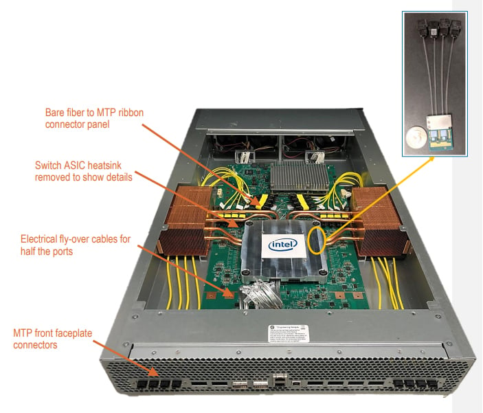
The CPO Optical Switching Module that Intel Demoed in 2020
The structure of the 1.6Tpbs PIC is shown in the figure below. The waveguide route is >30cm, >600 electrodes, and 4 temperature sensors. It includes:
Laser: 16*2 channels based on its own hybrid integrated laser; each channel has two backup lasers to improve the reliability of the x system.
Laser Selection Optical Switch: 16 heater-based 2×1 MZI structures
Silicon photonics micro-ring modulators: 16 silicon photonics micro-ring modulators with integrated thermal tuning that can achieve 106 Gbps PAM4 modulation.
MPD: 48 Germanium PDs, each supporting 106 Gbps PAM4 modulation signals.
Passive alignment technology: 16 integrated V-Grooves and SSC structure.
The picture below is its PIC-EIC platform, which includes all active devices, passive devices, and electrical chip structures.
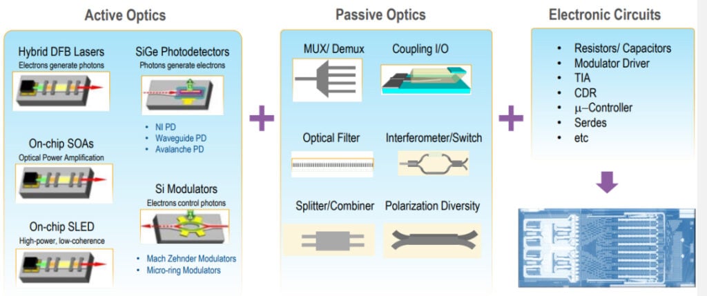
PIC-EIC Platform
SOA-on-chip is its unique technology that can achieve an output power of 100mW (20dBm) inside the waveguide with minimal loss, as shown in the figure below.
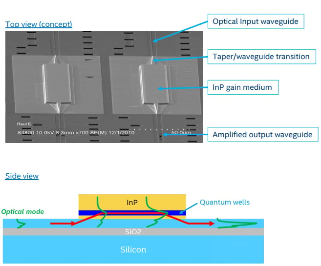
SOA Technology
The laser is based on III/V-Si Hybrid DFB lasers. The structure diagram is shown below. It can work from 0 to 150 degrees, so it can support Uncooled. The optical power is 25mW@80C@100mA, low RIN<-155dB/Hz, and high SMSR>40dB.
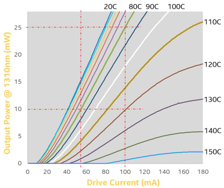
Laser Structure Diagram
The micro-ring modulator adopts an L-type doped PNJ structure, with high modulation efficiency (overlap and doping are optimized) <0.55Vcm@1310nm, extremely small size <20um, and high bandwidth 50 GHz EO BW (low series resistance and stray capacitance).
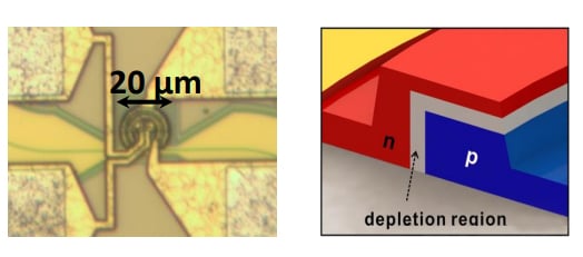
Micro-Ring Modulator
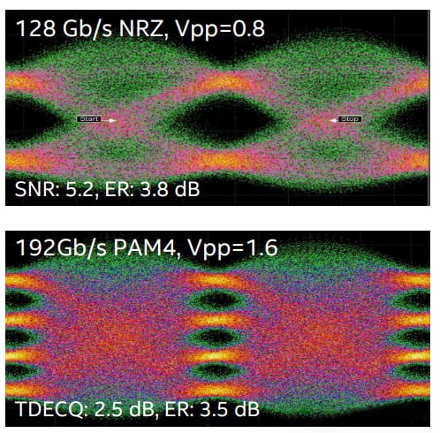
The figure below is eye diagram of its 128Gb/s NRZ micro-ring modulator with Vpp=0.8V, ER=3.8dB, which was the highest modulation rate achievable at the time.
Eye Diagram of Micro-ring Modulator
The biggest problem with the micro-ring modulator is the drift of the central wavelength. One type of drift is caused by environmental changes in actual work which Intel has its own unique monitoring technology and compensation methods to cope with. The other type is the drift of the central wavelength caused during process engineering. Intel has its own unique trimming technology, as shown in the figure below. During the manufacturing process, Ge doping is performed to compensate according to the wavelength offset, and ultimately wafer-level control of ±32pm can be achieved, which greatly reduces the power consumption of wavelength tuning.
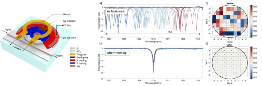
Trimming technology
For the fifth-generation optical IO, Intel has also made deployments that can realize 8Tb/sde bidirectional transmission, including 8-wave 64Gbps NRZ single fiber, 8 transmitters and 8 receivers, high-performance on-chip lasers and SOA, high-speed micro-ring modulators, high-speed Ge PD, and V-grooves fiber passive alignment technology. The figure below shows a multiplexed 8-wave 200GHz-spaced DFB array.
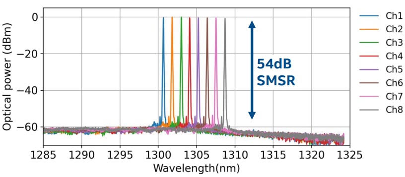
Multiplexed 8-wave 200GHz spacing DFB array
The figure below is Intel’s outlook on future optical IO. The 3D packaging structure of hybrid integrated chips is an inevitable trend. As shown in the figure below, the PIC is flipped on the EIC, and the EIC chip and the computing chip XPU are interconnected on the substrate through EMIB. The target power consumption is 3pJ/bit and each optical fiber transmits 1Tbps over a distance of >100m with latency<10ns.
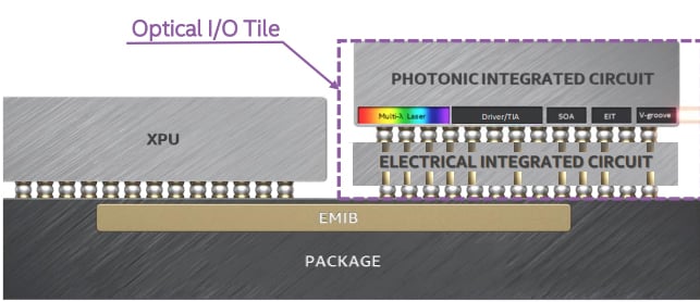
Intel’s Outlook on Future Optical IO
In summary, based on core IP, Intel has gradually realized 800G silicon photonic transceivers, CPO and Optical IO. We can tell that both CPO and Optical IO can give full play to the advantages of silicon photonic chips in terms of integration and power consumption, solve the pain points of chip bandwidth, and the 3D packaging structure of hybrid integrated chips may be the real field of application of III-V and silicon photonics.
Related Products:
-
 Intel Compatible 100G QSFP28 BIDI TX1304nm/RX1309nm Single Lambda LC SMF 30km PAM4 DDM Optical Transceiver Module
$1100.00
Intel Compatible 100G QSFP28 BIDI TX1304nm/RX1309nm Single Lambda LC SMF 30km PAM4 DDM Optical Transceiver Module
$1100.00
-
Intel Compatible 100G QSFP28 BIDI TX1309nm/RX1304nm Single Lambda LC SMF 30km PAM4 DDM Optical Transceiver Module
$1100.00
-
Intel E40GQSFPESR Compatible 40G QSFP+ ESR4 850nm 400m MTP/MPO MMF DDM Transceiver Module
$30.00
-
Intel E40GQSFPER Compatible 40G QSFP+ ER4 1310nm (CWDM4) 40km LC SMF DDM Transceiver Module
$449.00
-
Intel E40GQSFPLR Compatible 40G QSFP+ LR4 1310nm 10km MTP/MPO SMF DDM Transceiver Module
$149.00
-
Intel E40GQSFPSR Compatible 40G QSFP+ SR4 850nm 150m MTP/MPO MMF DDM Transceiver Module
$25.00