To further improve the optical coupling efficiency and output optical power of the optical module, FiberMall has designed and optimized the 400G QSFP-DD SR8. It utilizes passive components with lenses as crucial elements for optical coupling to enhance the coupling efficiency. The high-frequency circuits of the optical module are analyzed and optimized using the Input/Output Buffer Information Specification (IBIS) model. Finally, optical design, link simulation, and testing are performed on the optical module. The test results indicate that the designed optical transceiver module has a relatively clear eye diagram, with a jitter of around 2.3ps, and good consistency across channels, with no bit errors within 202s. No packet loss occurred after 100m signal transmission, and the system performance remained stable.
Overall Design of the Optical Module
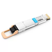
In 400G short-range optical transmission products, the demand for the 400G QSFP-DD SR8 optical module is the highest. Each optical module includes 16 transmission channels (8 transmitters and 8 receivers), with a transmission rate of 50Gb/s per channel. The signal modulation scheme is 4-level pulse amplitude modulation (PAM4), simultaneously satisfying the 400Gb/s rate for uplink and downlink transmissions. The circuit mainly includes a digital signal processor (DSP) chip, transimpedance amplifier (TIA) chip, and driver chip. In contrast, the optical path and passive optical components include a vertical-cavity surface-emitting laser (VCSEL) chip, a photodiode (PD) chip, and optical lenses.
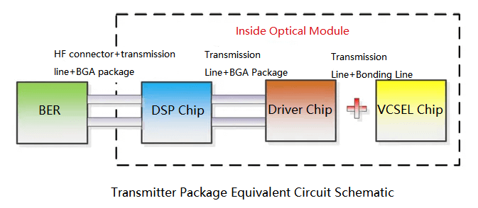
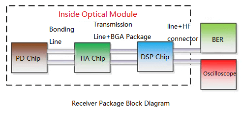
On the transmitter side, the electrical signal enters the PAM4 DSP chip through the electrical connector interface for signal conditioning. The processed high-frequency signal is then divided into two groups of 4-channel signals and enters the driver chip. The driver chip amplifies the signal and drives the VCSEL chip to perform electrical-to-optical conversion. On the receiver side, the optical signal enters the PD chip through the MPO16 optical interface, and the PD chip generates a photocurrent. The photocurrent is then amplified and amplitude-shaped by the TIA chip before entering the DSP chip. The high-frequency signal is conditioned and output in the DSP chip, completing the optical-to-electrical conversion.
In the manufacturing of the 400G QSFP-DD SR8 module, high-precision chip mounters are used to place the driver, TIA, VCSEL, and PD chips onto the printed circuit board (PCB). Then, a high-precision wire bonder is employed to connect the various chips, enabling the continuity of the circuit signals. During the wire bonding process, the wire loop height is reduced, significantly shortening the length of the bonding wires and minimizing the impact of high-speed signal reflections. On the transmitter side, the driver chip’s and VCSEL chip’s top surfaces are placed on the same horizontal plane. On the receiver side, the top surfaces of the TIA chip and PD chip are placed on the same horizontal plane, effectively shortening the length of the bonding wires. The gold-plated surface where the electrical chips are located has several through-holes that directly transfer heat to the backside openings of the PCB. Simultaneously, a high thermal conductivity material is filled on the backside and in contact with the metal housing, providing an ideal heat dissipation channel. Additionally, high thermal conductivity materials are filled in the gaps between the electrical chips and the metal housing, ensuring excellent thermal management performance. After completing the wire bonding of the optical path chips and electrical chips, passive components with added lenses are used for integrated optical coupling packaging on both the transmitter and receiver sides, completing the hermetic sealing of the optical engine. Compared to passive components without lenses, the coupling efficiency can be improved by 10% to 15% when using these passive components with added lenses.
High-Frequency Electrical and Optical Design of the 400G QSFP-DD SR8
PCB Design of the 400G QSFP-DD SR8
The PCB of the entire module adopts a 10-layer structure, with 4 layers for high-frequency differential lines and 6 layers for reference and DC layers. FiberMall utilizes impedance calculation software (Polar SI9000) and 3D signal simulation software HFSS to perform impedance calculations and simulations for the high-frequency differential lines (for the outer differential structure, the 100Ω impedance differential line width is 4mil, and the spacing is 8mil). During the PCB manufacturing process, the board material for the high-frequency differential signal layers must be a low dielectric constant, high-speed specialized material, with Rogers or Panasonic M6 being commonly used. Furthermore, to ensure the physical symmetry of the various layers and prevent PCB deformation due to uneven heating, the board materials need to be symmetrically treated. FiberMall’s optical module design employs ordinary FR4 material for the reference and DC routing layers.
The Goldfinger contacts and coupling capacitors cannot achieve complete continuity for high-frequency signals. Therefore, FiberMall optimized the high-frequency performance of the high-speed circuits from the module’s finger contacts to the DSP chip and from the DSP chip to the driver chip. The finger contact positions are designed according to the standard QSFP-DD Multi-Source Agreement (MSA), and gold and nickel-palladium-gold plating processes are employed to reinforce the finger contacts, enhancing their wear resistance and conductivity, and thereby reducing signal leakage. Additionally, by increasing the distance between the electrical reference planes surrounding the circuit and the signal vias, the inductance of the circuit is improved, reducing signal reflections. The local trimming method of the simulation software is used to trim and perform high-frequency simulations on the 16 pairs of high-frequency lines from the finger contacts to the DSP chip. In combination with impedance calculation software, adjustments are made to the line thickness, line width, and line spacing for each group of high-frequency lines. When addressing the coupling capacitors, the distance is primarily adjusted based on the simulation results, and reference ground layer holes are drilled at the four corners of the entire model to form a return path for interference signals, achieving anti-interference capabilities.
The high-frequency optimization results show that all 32 groups of high-speed differential lines, both transmitting and receiving, can achieve a 3dB bandwidth greater than 35GHz (the actual bandwidth used does not exceed 20GHz). The impedance values of all high-frequency lines are controlled at 100Ω (with an accuracy of 1Ω), and the return loss values of all high-frequency lines are less than -15dB. Furthermore, the VCSEL chip is connected to the driver chip through differential bonding wires, using conventional 25μm diameter gold wires. The longest bonding wire is shortened from 500μm to 280μm, reducing the insertion loss by 0.3dB.
The optimization of the high-frequency differential lines on the receiver side is roughly similar to that of the transmitter side, employing the trimming method to trim, correct, simulate, optimize, and then re-correct each pair of differential lines until the desired differential lines are obtained. After optimization, the impedance of all differential lines is precisely controlled at 100Ω (accuracy ±1Ω), the 3dB bandwidth meets the 35GHz requirement, and the return loss is less than -8dB.
400G QSFP-DD SR8 Optical Design
Using placement equipment, the Driver chip and TIA chip are array-mounted according to the designed mounting position markings, ensuring that the mounting position error of the two chips is less than 3μm, thereby ensuring the accuracy and stability of optical coupling of the product. After the Driver chip and TIA chip are mounted, the VCSEL chip and PD chip are mounted, corresponding to the working areas of the Driver chip and TIA chip, respectively, and aligned according to the pin positions of the GSG, with a mounting error of less than 3μm. After the mounting is completed, the wire bonding machine parameters are set according to the wire length and angle obtained from the simulation, and wire bonding is performed for all pins, thus completing the wire bonding work between the chips and the PCB.
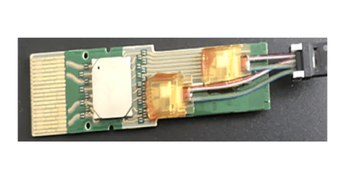
After the wire bonding is completed, FiberMall uses a high-precision coupling machine to perform active coupling on the module. The coupling work is carried out in two steps: one step is to couple one set of array-mounted Driver and TIA chips (using an optical power meter to detect the transmitted optical power of 4 TX channels and using software to detect the receiving response of 4 RX channels). When the detection indicators of transmission and reception reach the maximum value simultaneously, the Lens is fixed with glue. The other step is to couple and fix the other set of chips in the same way. The physical 400G QSFP-DD SR8 module made by FiberMall is shown in the figure.
Optical Module Simulation
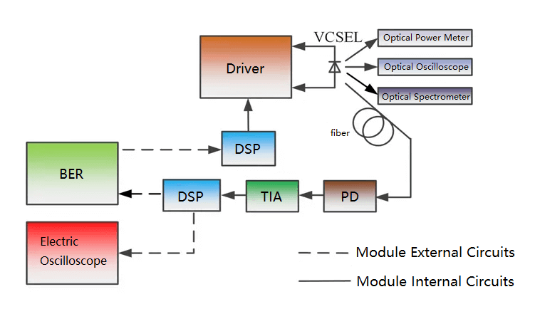
Optical Module Link Simulation Structure
The following figure shows the schematic diagram of the optical module link simulation structure. At the transmitting end, the VCSEL emits a beam of light under the driving of the Driver chip, and the high-speed RF signal output by the Driver chip modulates the optical signal and outputs it. An optical power meter, optical oscilloscope, and optical spectrum analyzer can obtain important parameters such as average optical power (Pawg), extinction ratio (ER), and wavelength of the optical signal. When performing module self-loopback or cross-testing, the optical fiber receives the optical signal at the receiving end. After a series of signal processing by chips such as PD, TIA, and DSP, the signal is transmitted to an electrical oscilloscope, where the converted electrical signal eye diagram can be observed and the signal quality analyzed. By inputting this electrical signal into the RX port of a bit error rate tester, the bit error rate tester can read the real-time bit error rate to determine whether the transmission quality of the module meets international standard requirements.
400G QSFP-DD SR8 Optical Module Testing
FiberMall performed eye diagram testing and bit error rate measurement on the 400G optical transceiver module. The eye diagram and bit error rate plot are shown in Figures 8 and 9, respectively. The test results show that the module’s eye diagram is relatively clear, with an eye diagram jitter of around 2.3ps, and the channels have good consistency, with no bit errors within 202s. Additionally, FiberMall tested the system transmission performance of the 400G optical transceiver module over a transmission distance of 100m. It was found that the eye diagrams of the channels did not differ much from the direct connection test results. Although the average jitter increased slightly, the channel eye diagram consistency remained good, and no packet loss occurred at a transmission rate of 50Gb/s, indicating a relatively stable system performance. The total power consumption of the entire optical module is 9.8W, with low power consumption.
Conclusion
FiberMall has systematically designed the structure and high-frequency circuits for the 400G QSFP-DD SR8 and optimized them using professional software. The test results show that compared to passive devices without lenses, using passive devices with added lenses can increase the coupling efficiency by 10% to 15%. After optimization of the high-frequency lines, the return loss values are all less than -15dB, and the insertion loss has decreased by 0.3dB. The eye diagram of the optical transceiver module is clear, with a jitter of approximately 2.3ps, and the channels have good consistency, with no bit errors within 202s. After 100m of signal transmission, the bit error rate is less than 1E-12, and the total power consumption of the module is 9.8W, meeting international standard requirements.
Related Products:
-
 QSFP-DD-400G-SR8 400G QSFP-DD SR8 PAM4 850nm 100m MTP/MPO OM3 FEC Optical Transceiver Module
$149.00
QSFP-DD-400G-SR8 400G QSFP-DD SR8 PAM4 850nm 100m MTP/MPO OM3 FEC Optical Transceiver Module
$149.00
-
Cisco QDD-400G-SR8-S Compatible 400G QSFP-DD SR8 PAM4 850nm 100m OM4 MPO-16 DDM MMF Optical Transceiver Module
$149.00
-
Arista Networks QDD-400G-SR8 Compatible 400G QSFP-DD SR8 PAM4 850nm 100m MTP/MPO OM3 FEC Optical Transceiver Module
$149.00
-
DELL 400G-Q56DD-SR8 Compatible 400G QSFP-DD SR8 PAM4 850nm 100m MTP/MPO OM3 FEC Optical Transceiver Module
$149.00
-
EdgeCore ET7502-SR8 Compatible 400G QSFP-DD SR8 PAM4 850nm 100m OM4 MPO-16 DDM MMF Optical Transceiver Module
$149.00
-
H3C QSFPDD-400G-SR8-MM850 Compatible 400G QSFP-DD SR8 PAM4 850nm 100m MTP/MPO OM3 FEC Optical Transceiver Module
$149.00