SambaNova Systems hailed as one of the top ten unicorn companies in the United States, raised $678 million in a Series D funding round led by SoftBank in April 2021, achieving a staggering $50 billion valuation. The company’s previous funding rounds involved prominent investors such as Google Ventures, Intel Capital, SK, Samsung Catalyst Fund, and other leading global venture capital firms. What disruptive technology has SambaNova developed to attract such widespread interest from top-tier investment institutions worldwide?
According to SambaNova’s early marketing materials, the company has taken a different approach to challenge the AI giant NVIDIA.
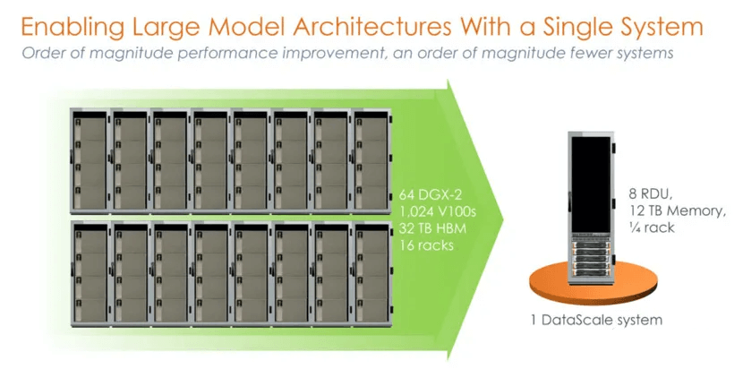
The comparison is quite astonishing: a single SambaNova machine is claimed to be equivalent to a 1024-node NVIDIA V100 cluster built with tremendous computational power on the NVIDIA platform. This first-generation product, based on the SN10 RDU, is a single 8-card machine.
Some might argue that the comparison is unfair, as NVIDIA has the DGX A100. SambaNova seems to have acknowledged this, and their second-generation product, the SN30, presents a different comparison:
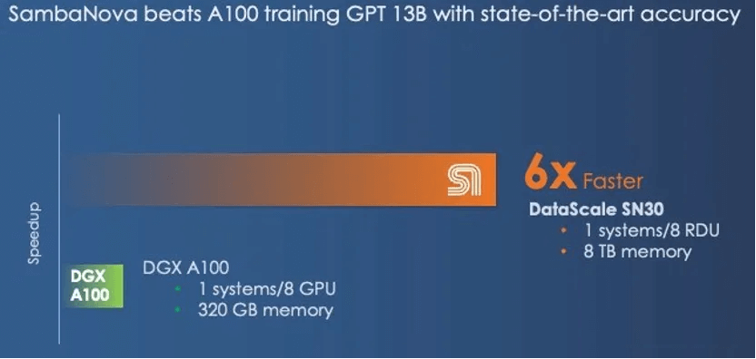
The DGX A100 offers 5 petaFLOPS of computing power, while SambaNova’s second-generation DataScale also delivers 5 petaFLOPS. In terms of memory, the DGX A100 has 320GB of HBM, while the SN30 boasts 8TB of DDR4 (the author speculates that this might be a typo, and the actual figure should be 3TB * 8).
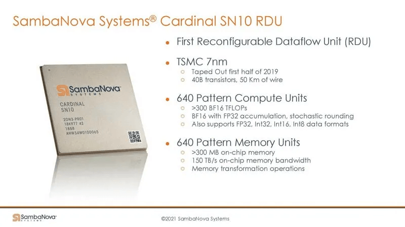
The second-generation chip is a Die-to-Die version of the SN10 RDU. The SN10 RDU’s architecture specifications are 320TFLOPS@BF16, 320M SRAM, and 1.5T DDR4. The SN30 RDU essentially doubles these specifications, as described below:
“This chip had 640 pattern compute units with more than 320 teraflops of compute at BF16 floating point precision and also had 640 pattern memory units with 320 MB of on-chip SRAM and 150 TB/sec of on-chip memory bandwidth. Each SN10 processor was also able to address 1.5 TB of DDR4 auxiliary memory.”
“With the Cardinal SN30 RDU, the capacity of the RDU is doubled, and the reason it is doubled is that SambaNova designed its architecture to make use of multi-die packaging from the get-go, and in this case SambaNova is doubling up the capacity of its DataScale machines by cramming two new RDU – what we surmise are two tweaked SN10s with microarchitectures changes to better support large foundation models – into a single complex called the SN30. Each socket in a DataScale system now has twice the compute capacity, twice the local memory capacity, and twice the memory bandwidth of the first generations of machines.”
High bandwidth and large capacity are mutually exclusive choices. NVIDIA opted for high bandwidth with HBM, while SambaNova chose large capacity with DDR4. From a performance perspective, SambaNova appears to outperform NVIDIA in AI workloads.
SambaNova SN10 RDU at Hot Chips 33
The Cardinal SN10 RDU is SambaNova’s first-generation chip, while the SN30 is the second-generation chip (a Die-to-Die version of the SN10). We notice its significant features, including a large on-chip SRAM, massive on-chip bandwidth, and an enormous 1.5T DRAM capacity.
The SN40L is the third-generation chip (with added HBM). The first two generations of chips relied on the Spatial programming characteristics of Dataflow, reducing the demand for high DRAM bandwidth and opting for the large-capacity DDR route. However, the third-generation chip builds upon this foundation and incorporates 64GB of HBM, combining both bandwidth and capacity.
This leads to an interesting topic: how to scale the system, especially when organizing such a large DRAM capacity, and why DDR4 was chosen over other options.
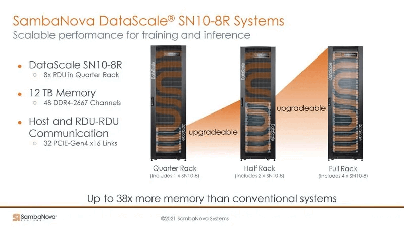
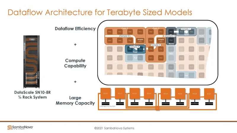
According to the introduction, the SN10-8R has eight cards occupying 1/4 of a rack. Each RDU contains six Channel Memory, with each channel having 256GB. An SN10-8R has 48 channels, totaling 12TB, using DDR4-2667 per channel, and the Q&A also mentioned DDR4-3200.
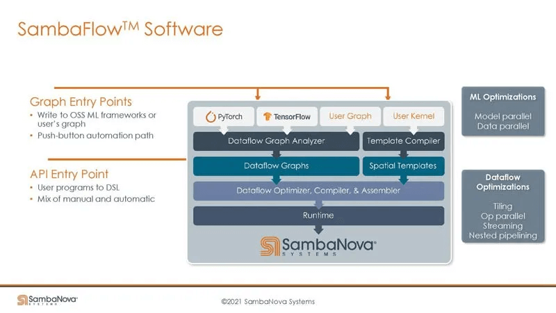
Furthermore, the software stack is compatible with mainstream AI frameworks. The Dataflow Graph Analyzer constructs sub-graphs suitable for scheduling and deployment on the RDU from the original DAG, forming the Dataflow Graph.
The Dataflow Compiler compiles and deploys based on the Dataflow Graph, invoking the operator template library (Spatial Templates), similar to the P&R tool in EDA, deploying the Dataflow Graph onto the RDU’s hardware computing and storage units.
Additionally, SambaNova provides a way for users to customize operators, supporting user-defined operators based on their needs. The author speculates that this is based on the C+Intrinsic API provided by LLVM, as the SN10 core architecture includes many SIMD instructions, likely requiring manual coding.
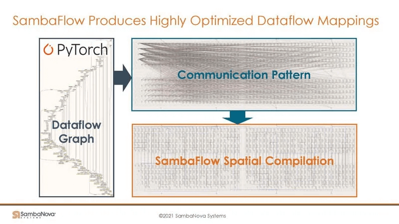
On reconfigurable hardware, communication is also programmable, a point strongly emphasized by another architecture, Groq.
Compared to traditional architectures, the author’s personal understanding is that the benefits of this approach in SambaNova’s architecture are:
1. The Spatial programming paradigm has more regular communication patterns, which can be software-controlled. In contrast, traditional approaches have more chaotic communication patterns, leading to potential congestion.
2. With an enormous DRAM capacity, more data can be stored on-card, converting some inter-card communication to on-card DRAM data exchange, reducing communication overhead and lowering the demand for inter-card communication bandwidth.
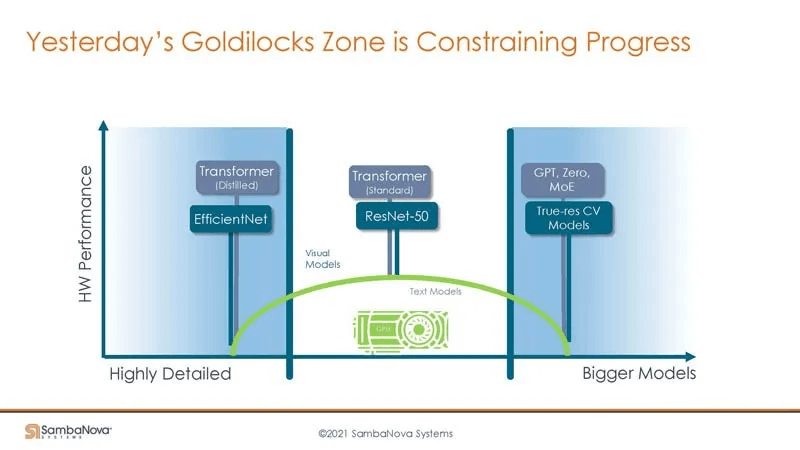
GPUs excel at certain specific applications, but for very large models that cannot fit or run efficiently on a single GPU, their performance can suffer.
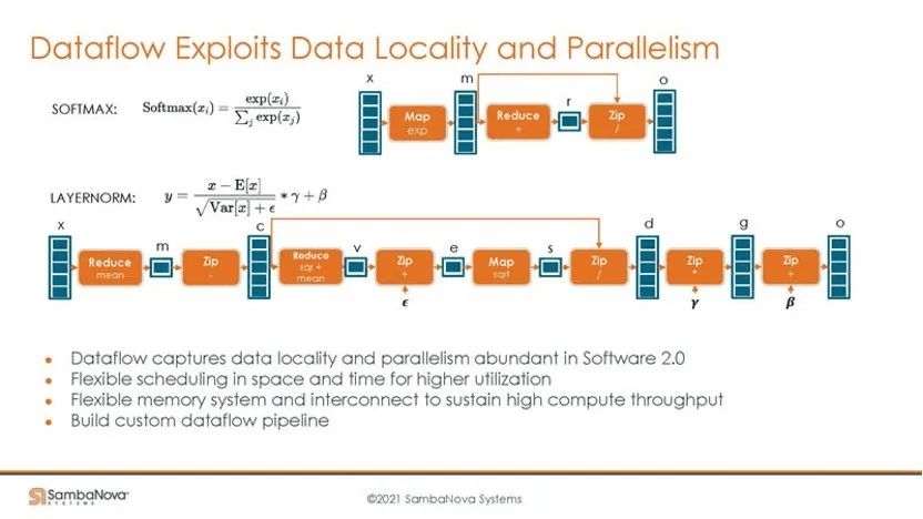
SambaNova’s dataflow architecture features numerous compute PCUs (0.5 TOPS) and storage PMUs (0.5M), which can be leveraged for parallel and data locality optimizations. The example below illustrates how chaining multiple PCUs enables fine-grained pipeline parallelism, with PMUs facilitating data exchange between PCUs and providing ideal data locality control.
Potential Issues
Regular Data Parallelism: Operations like Parallel.For require a shared memory for data exchange. In SN10 and SN30, is this limited to DDR? In SN40L, HBM can be used, potentially improving latency.
PCU and PMU Granularity: The granularity of PCUs and PMUs is very fine. How is the DAG decomposed to this level?
(A) Does the Dataflow Graph Analyzer directly decompose to this fine granularity, with operators then interfacing with it?
(B) Or does the Dataflow Graph Analyzer decompose to a coarser granularity, with operators controlling hardware resources and a coarse-grained operator being hand-written to interface?
In my opinion, the graph layer provides a global view, enabling more optimization opportunities. However, a powerful automatic operator generation tool is needed to codegen operators from the subgraphs produced by the Dataflow Graph Analyzer using minimal resources. Hand-writing operators would be challenging for flexible graph-layer compilation. I speculate that the real-world approach might involve hand-writing operators for fixed patterns, with the graph layer’s Dataflow Graph Analyzer compiling based on these existing patterns, similar to most approaches.
Fully exploiting the performance potential is a significant challenge. SambaNova’s architecture allows hardware reconfiguration to adapt to programs, unlike traditional architectures where programs must adapt to hardware. Combined with fine-grained computing and storage, this provides a larger tuning space.
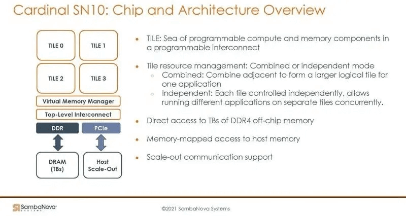
The SN10 architecture, as shown in the image, consists of Tiles made up of programmable interconnects, computing, and memory. Tiles can form larger logical Tiles, operate independently, enable data parallelism, or run different programs. Tiles access TB-level DDR4 memory, host machine memory, and support multi-card interconnects.
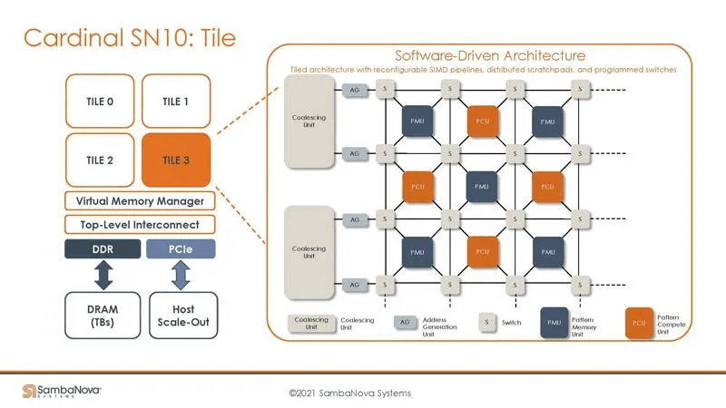
Tiles in the SambaNova architecture are composed of three programmable units: Switch, PCU (Programmable Compute Unit), and PMU (Programmable Memory Unit). Understanding how to control these units is crucial for engineers writing operators.
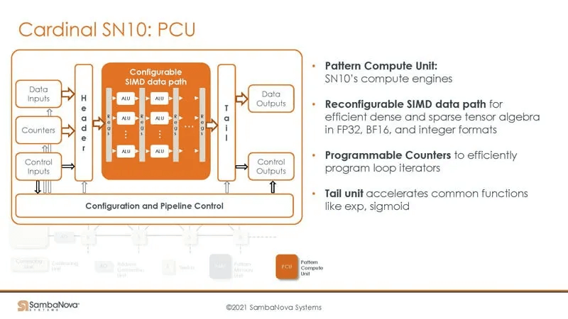
The PCU is primarily composed of configurable SIMD instructions. Programmable counters to execute inner loops in programs. A Tail Unit to accelerate transcendental functions like Sigmoid Funtion.
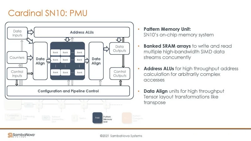
The PMU is a multi-banked SRAM that supports tensor data format conversions, such as Transpose.
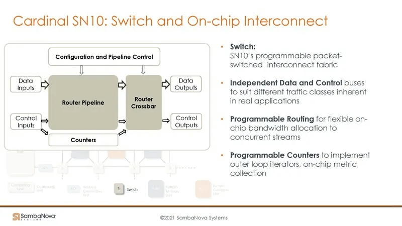
The Switch contains a Router Pipeline and a Router Crossbar, controlling data flow between PCUs and PMUs. It includes a counter to implement outer loops.
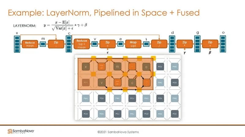
Here’s an example of using Layer Normalization, outlining the different computation steps. On the SambaNova hardware, the Switch connects different PCUs and PMUs to form pipelines. Nearby computations can rapidly exchange data through PMUs (a form of in-memory computing) while supporting concurrent pipelines (if the program has parallel DAGs).
Note that this example follows a spatial programming paradigm, where different compute units execute unique computation programs (PCUs execute the same program at different times). Computations are fully unrolled in the spatial dimension, with some fusion applied.
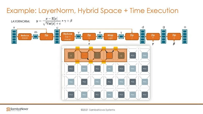
Building upon the Space, a temporal programming approach can be added to process data using minimal PMUs, MCUs, and Switches. The temporal approach considers executing specific programs on specific data at particular times. Intuitively, the same compute unit may execute different programs at different times. This approach uses fewer hardware resources, allowing the chip to execute more programs. Combined with high-speed on-chip interconnects and large DDR4 capacity, larger-scale programs can be processed. Both spatial and temporal programming modes are essential.
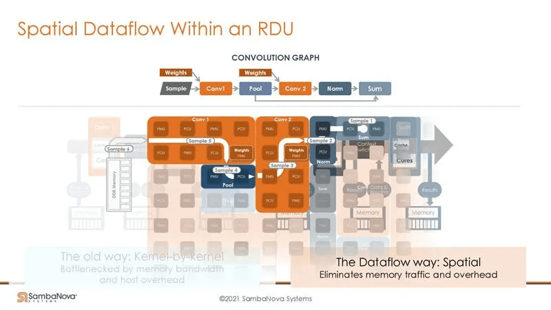
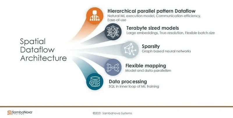
The following is a coarse-grained execution process for a small network, while the previous example focused on a Layer Normalization operator. Unlike other architectures (TPUs, Davinci), the SambaNova architecture natively supports on-chip fusion.
With 1/4 of a rack providing 12TB of DRAM, there is sufficient capacity to fully utilize the chip’s compute power. The SN40L further adds 64GB of HBM, likely placed between the DDR4 and PMU SRAM based on the PR content.
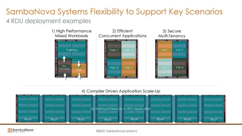
Such an architecture requires extremely powerful compilation techniques to support it, heavily relying on the compiler to map the dataflow graph onto the hardware resources. The following are various deployment scenarios that require compiler support.
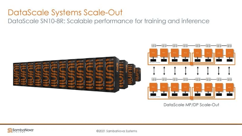
Multi-Card and Multi-Machine Interconnected Systems for Training and Inference
The benefit of using a large DRAM capacity is that it can support training 1 Trillion Parameter Language Models without the need for model partitioning, unlike GPU systems. Here’s a comparison: training a 1T model on GPUs requires complex model parallelism techniques, while on the SambaNova system, the footprint is smaller. This raises an interesting point: Cerebras’ Dojo wafer-scale technology also aims to reduce the compute footprint. Perhaps building upon SambaNova’s current work, their cores could be implemented using a wafer-scale approach similar to Cerebras Dojo (SambaNova’s PCUs and PMUs are also relatively fine-grained). Conversely, other architectures could consider SambaNova’s large DRAM capacity approach (these architectures also have large SRAMs and are dataflow-based).
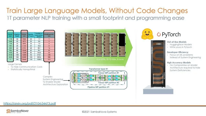
The significance of reducing the footprint can be appreciated from Elon Musk’s statement. Enabling GPU clusters above 10K is a substantial undertaking, with difficulty and workload comparable to supercomputers, raising the technical barrier significantly. If the FSD 12 proves the viability of the end-to-end large model approach for autonomous driving, the availability of large compute clusters will become crucial for companies pursuing this technology.
In the absence of H100 availability, meeting the training demands of large models for domestic leading automakers could quickly become a bottleneck.

One of SambaNova’s other advantages is that it can support training on high-resolution images like 4K or even 50K x 50K without needing to downsample to a lower precision. If applied in the self-driving domain, training on high-definition video can provide accuracy advantages.
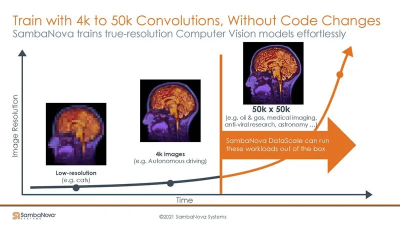
On GPUs, downsampling is generally required (possibly first on the host CPU) to fit the data into the GPU’s DRAM. SambaNova’s large memory capacity means no downsampling or splitting is needed.
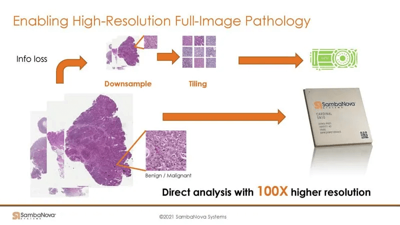
Supporting training on higher resolution images implies a need for higher training precision.
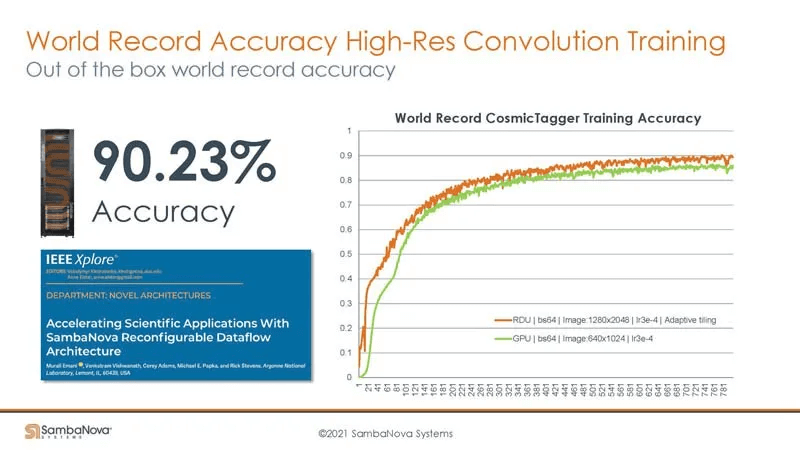
Similarly, for recommendation models, accuracy improvements translate to massive economic gains. SambaNova’s large memory architecture is highly beneficial for boosting recommendation model accuracy.
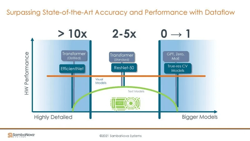
Here is SambaNova’s acceleration effect across different model scales:
Summary
The RDU’s Dataflow architecture enables model execution on SRAM, reducing DRAM bandwidth demands. However, it also requires the compiler to deploy the Dataflow Graph onto the RDUs.
The compiler uses a combined time+space technique to maximize hardware utilization for larger programs. Combined with high DRAM capacity, this supports larger models and high-resolution image training.
Interpreting the SN40L Architecture Changes
“SambaNova’s SN40L chip is unique. It addresses both HBM (High Bandwidth Memory) and DRAM from a single chip, enabling AI algorithms to choose the most appropriate memory for the task at hand, giving them direct access to far larger amounts of memory than can be achieved otherwise. Plus, by using SambaNova’s RDU (Reconfigurable Data Unit) architecture, the chips are designed to efficiently run sparse models using smarter compute.”
The new SN40L architecture released in early September 2023 added more compute cores and introduced HBM for the first time. This section attempts to interpret the reasoning behind this choice.
For inference, large language model parameters are tens to hundreds of GBs, and the KV cache is also tens to hundreds of GBs, while a single SN40 card’s SRAM is just a few hundred MBs (the SN10 was 320MB).
For example, with the 65B parameter LLaMA model, storing the weights in FP16 format requires 65G*2=130GB. Taking LLaMA-65B as an example again, if the inference token length reaches the maximum of 2048 allowed by the model, the total KV cache size will be as high as 170GB.
Ideally, parameters would reside in SRAM, the KV cache in memory close to compute, and inputs would stream directly on-chip to drive the compute pipeline. Obviously, a few hundred MB of SRAM per card is insufficient to host 100+GB of parameters while leaving room for inputs, even with multiple interconnected chips requiring thousands of chips. To reduce the footprint, a time-multiplexed programming model is still needed to reuse on-chip compute resources, loading different programs at different times, requiring weight streaming with different weights for different layers. However, if weights and the KV cache are stored in DDR, the latency would be quite high, making HBM an excellent medium for hosting hot data (weights, KV cache, or intermediate data that needs to spill).
DDR is used for parameters and input data, while HBM acts as an ultra-large cache for hot data (weights, KV cache, or intermediate data about to be used).
For fine-tuning and training, the bandwidth requirements are even greater. Introducing HBM provides increased bandwidth and capacity benefits.
Related Products:
-
 OSFP-800G-FR4 800G OSFP FR4 (200G per line) PAM4 CWDM Duplex LC 2km SMF Optical Transceiver Module
$5000.00
-
 OSFP-800G-2FR2L 800G OSFP 2FR2 (200G per line) PAM4 1291/1311nm 2km DOM Duplex LC SMF Optical Transceiver Module
$4500.00
-
 OSFP-800G-2FR2 800G OSFP 2FR2 (200G per line) PAM4 1291/1311nm 2km DOM Dual CS SMF Optical Transceiver Module
$4500.00
-
 OSFP-800G-DR4 800G OSFP DR4 (200G per line) PAM4 1311nm MPO-12 500m SMF DDM Optical Transceiver Module
$3500.00
-
 NVIDIA MMS4X00-NM-FLT Compatible 800G Twin-port OSFP 2x400G Flat Top PAM4 1310nm 500m DOM Dual MTP/MPO-12 SMF Optical Transceiver Module
$1200.00
-
 NVIDIA MMA4Z00-NS-FLT Compatible 800Gb/s Twin-port OSFP 2x400G SR8 PAM4 850nm 100m DOM Dual MPO-12 MMF Optical Transceiver Module
$850.00
-
 NVIDIA MMS4X00-NM Compatible 800Gb/s Twin-port OSFP 2x400G PAM4 1310nm 500m DOM Dual MTP/MPO-12 SMF Optical Transceiver Module
$1100.00
-
 NVIDIA MMA4Z00-NS Compatible 800Gb/s Twin-port OSFP 2x400G SR8 PAM4 850nm 100m DOM Dual MPO-12 MMF Optical Transceiver Module
$750.00
-
 NVIDIA MMS1Z00-NS400 Compatible 400G NDR QSFP112 DR4 PAM4 1310nm 500m MPO-12 with FEC Optical Transceiver Module
$800.00
-
 NVIDIA MMS4X00-NS400 Compatible 400G OSFP DR4 Flat Top PAM4 1310nm MTP/MPO-12 500m SMF FEC Optical Transceiver Module
$800.00
-
 NVIDIA MMA1Z00-NS400 Compatible 400G QSFP112 SR4 PAM4 850nm 100m MTP/MPO-12 OM3 FEC Optical Transceiver Module
$650.00
-
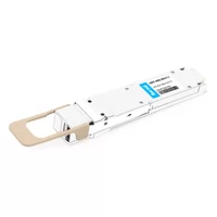 NVIDIA MMA4Z00-NS400 Compatible 400G OSFP SR4 Flat Top PAM4 850nm 30m on OM3/50m on OM4 MTP/MPO-12 Multimode FEC Optical Transceiver Module
$650.00
-
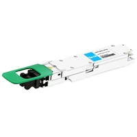 NVIDIA MMS4X50-NM Compatible OSFP 2x400G FR4 PAM4 1310nm 2km DOM Dual Duplex LC SMF Optical Transceiver Module
$1350.00
-
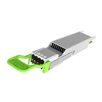 OSFP-XD-1.6T-4FR2 1.6T OSFP-XD 4xFR2 PAM4 1291/1311nm 2km SN SMF Optical Transceiver Module
$17000.00
-
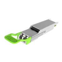 OSFP-XD-1.6T-2FR4 1.6T OSFP-XD 2xFR4 PAM4 2x CWDM4 2km Dual Duplex LC SMF Optical Transceiver Module
$22400.00
-
 OSFP-XD-1.6T-DR8 1.6T OSFP-XD DR8 PAM4 1311nm 2km MPO-16 SMF Optical Transceiver Module
$12600.00
