AI scenarios require optical modules to have the following features: low power consumption, large bandwidth, low latency, high reliability, and intelligence. Large bandwidth refers to the processing of high-speed signals, including the processing of optical and electrical signals. These parameters are interrelated. For example, high-speed EML requires the design of a large optical bandwidth on the one hand, and the processing of electrical signals (that is, RF signals) on the other hand. The resistors and capacitance used for impedance matching are to absorb the tail electromagnetic waves and avoid noise generated by the electrical signal echo. It is also necessary to avoid interference between the echo and the original signal wave.
MPD was used for DDM in the early years, but now it can also become an auxiliary judgment parameter for intelligentization. By monitoring the working status of the EML in real time, collecting the bias current and temperature, and drawing a curve that changes over time, we can analyze the degree of degradation of the EML’s current working state compared to its early stage, and whether it is about to fail, thus avoiding the interruption of AI calculations in large models.
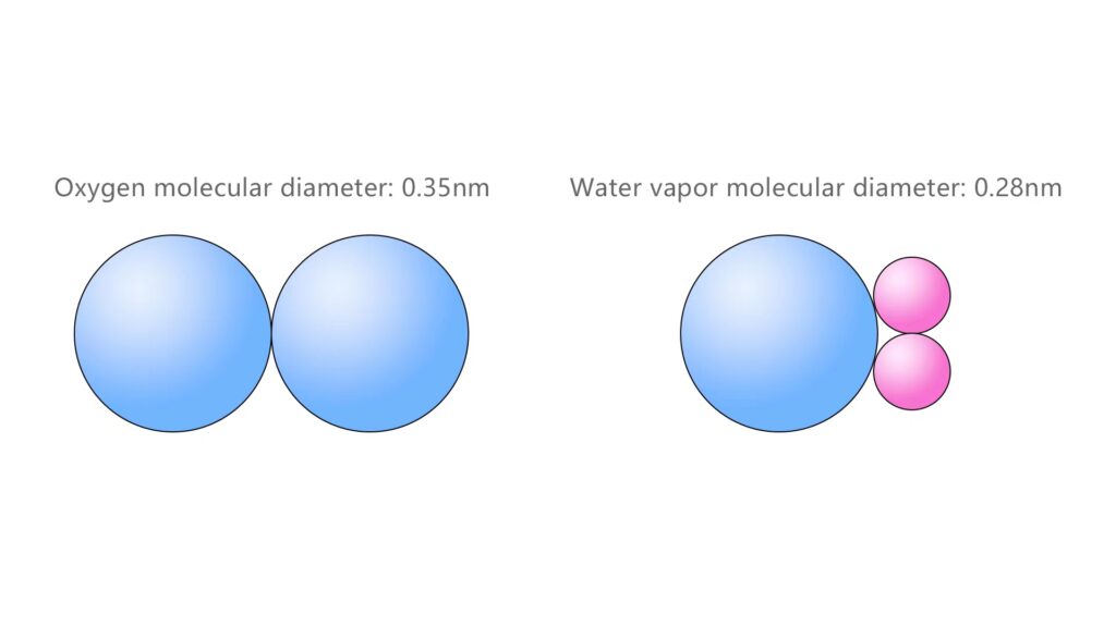
EML’s 800G optical transceiver does not need to be airtight in traditional data centers, but it needs to be airtight in AI scenarios. Why do we need to measure water content to make it airtight? This is because the core of airtightness is to achieve watertightness, avoiding chemical reactions between oxygen atoms in water molecules and InP compounds in EML. Oxygen molecules are larger than water molecules. If you can block water, you can also block oxygen.

Airtight is actually watertight
However, oxygen can be easily driven away, but water molecules cannot be avoided. For example, when metal plating is done in an electroplating process in an electrolyte, it is easy to produce water residue.
The exposure of DRV and TIA’s electrical chips, COB process, aluminum pads to the air, aluminum oxidation and residual water molecules form an “electrochemical” corrosion environment, causing reliability risks.
The VCSEL multi-mode module used in AI scenarios has a side oxidation process in the design of the VCSEL’s light-emitting aperture and current aperture. The oxidation, which is also a chemical reaction between aluminum and oxygen, is also a source of reliability risk.
Back to the large-bandwidth RF signal, the EML package has resistors capacitance to absorb and bypass the tail electromagnetic waves, but the contact between the gold finger inserted into the socket and the reed does not have this convenience. The reflection of tail electromagnetic wave is superimposed on the original signal, which produces jitter on the one hand and RIN noise on the other. In the worst case scenario, the reflected wave and the original wave will interfere and the signal will be useless. Therefore, controlling the resonance of parasitic parameters is an inevitable task for 800G and 1.6T.
Let’s go back to EML packaging. The traditional process is to use gold wire for electrical signal interconnection. Metal has a parasitic inductance, which can easily cause resonance. For EML’s large-bandwidth packaging, some manufacturers are trying their best to reduce this parasitic inductance, while some manufacturers directly replace the process and choose the Flip Chip structure without gold wire bonding process.
EML has bonding wire length, which will affect the high-speed signal bandwidth. VCSEL also has the same dilemma, so there are two sets of processes: VCSEL gold wire process and Flip chip process. The flip chip VCSEL requires a transparent substrate. Generally, glass is chosen, and the optical and radio frequency properties of the glass are brought out. This is the process of TGV and COG. In the TGV control group, you will see many people analyzing the pros and cons of TSV, TGV, and TMV, which is mainly about the relationship between the signal’s dielectric loss and bandwidth.
When talking about optical signals, compounds are often mentioned. InP and GaAs are both compounds, and their reliability is related to the destruction of oxygen. Copper is often mentioned for electrical signals, especially high-frequency/radio frequency electrical signals with large bandwidth. Copper is everywhere in optical transceivers.
The copper clad board of PCB, the smooth copper on the bare board, the reverse copper, and the rough copper, whose reliability need to be considered. The process of the source of copper, chemical copper deposition on copper cladding, electroplated copper, and the process between copper layers need to be carefully controlled.
Optical transceivers must be adapted to the optical fiber. The optical fiber is made of glass which is easy to crack during the end face contact process. On the one hand, it affects the optical signal; on the other, water molecules will be stored in the gaps, causing a reaction between silicon oxide and hydrogen-oxygen bonds. The adsorbed water vapor will absorb light of a specific wavelength.
This topic is related to the packaging technology and reliability.
It’s costly and of poor reliability to use optical fiber in optical transceivers, so it would be better to replace it with copper cable, DAC or AEC. Active cables use various copper wires, such as oxygen-free copper, which is much discussed nowadays. The so-called oxygen-free copper focuses on copper, not oxygen-free, reducing impurities in copper alloys, using pure copper, reducing RF losses, and lowering impedance. It’s just that pure copper can be single crystal or polycrystalline, and the latter one is cheaper. The gaps between grain boundaries will absorb oxygen and water vapor, which will then undergo oxidation reactions and cause cracks.
The essence of hermetic packaging of optical transceivers is to provide an “oxygen-free” cavity for the optical chip to improve reliability. Oxygen-free copper also improves reliability by placing copper in an oxygen-free environment. Only if it works reliably can the large bandwidth designed into optical transceiver be put to good use.
