HBM, or high-bandwidth memory, consists of multiple layers of DRAM Die stacked vertically. Each layer of Die is connected to the logic Die through TSV (through silicon via) technology, allowing 8-layer and 12-layer Die to be packaged in a small space. This achieves compatibility between small size and high bandwidth and high transmission speed, making it the mainstream solution for high-performance AI server GPU memory.
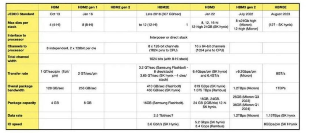
The current extended version of HBM3, HBM3E, provides a transmission speed of up to 8Gbps and 16GB of memory. It was first released by SK Hynix and will be mass-produced in 2024.
The main application scenario of HBM is AI servers. The latest generation of HBM3e is installed on the H200 released by NVIDIA in 2023. According to Trendforce’s data, AI server shipments reached 860,000 units in 2022, and it is expected that AI server shipments will exceed 2 million units in 2026, with a compound annual growth rate of 29%.
The growth in AI server shipments has catalyzed an explosion in HBM demand, and with the increase in the average HBM capacity of servers, it is estimated that the market size will be approximately US$15 billion in 25 years, with a growth rate of more than 50%.
HBM suppliers are mainly concentrated in the three major storage manufacturers SK Hynix, Samsung and Micron. According to Trendforce’s data, SK Hynix’s market share is expected to be 53% in 2023, Samsung’s market share is 38%, and Micron’s market share is 9%. The main changes in HBM process reflect on CoWoS and TSV.
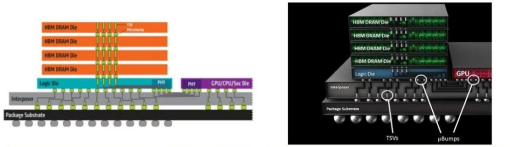
HBM principle diagram
HBM1 was first launched by AMD and SK Hynix in 2014 as a competitor to GDDR. It is a 4-layer die stack that provides 128GB/s bandwidth and 4GB of memory, which is significantly better than GDDR5 of the same period.
HBM2 was announced in 2016 and officially launched in 2018. It is a 4-layer DRAM die, but now it is mostly an 8-layer die, providing 256GB/s bandwidth, 2.4Gbps transmission speed, and 8GB memory; HBM2E was proposed in 2018 and officially launched in 2020. It has made significant improvements in transmission speed and memory, providing 3.6Gbps transmission speed and 16GB memory. HBM3 was announced in 2020 and officially launched in 2022. The number of stacked layers and management channels have increased, providing a transmission speed of 6.4Gbps, a transmission speed of up to 819GB/s, and 16GB memory. HBM3E is an enhanced version of HBM3 released by SK Hynix, providing a transmission speed of up to 8Gbps, a capacity of 24GB, which is planned to be mass-produced in 2024.
HBM Evolution Paths of the Three Major Storage Manufacturers
HBM is widely used in AI server scenarios due to its high bandwidth, low power consumption, and small size. The application of HBM is mainly concentrated in high-performance servers. It was first implemented in the NVP100 GPU (HBM2) in 2016, and then applied to V100 (HBM2) in 2017, A100 (HBM2) in 2020, and H100 (HBM2e/HBM3) in 2022. The latest generation of HBM3e is installed on the H200 released by NVIDIA in 2023, providing faster speed and higher capacity for servers.
HBM suppliers are mainly concentrated in three major manufacturers: SK Hynix, Samsung, and Micron, with SK Hynix leading the way. The three major storage manufacturers are mainly responsible for the production and stacking of DRAM Dies, and are competing in technology upgrades. Among them, the world’s first HBM released by SK Hynix and AMD was the first to supply the new generation of HBM3E in 2023, establishing its market position first. It mainly supplies NVIDIA, and Samsung supplies other cloud manufacturers. According to TrendForce data, in 2022, SK Hynix’s market share was 50%, Samsung’s market share 40%, and Micron’s market share about 10%.
HBM’s changes in packaging technology are mainly in CoWoS and TSV.
1) CoWoS: DRAM Die is placed together on a silicon interposer and connected to the underlying substrate through a ChiponWafer (CoW) packaging process. That is, the chip is connected to the silicon wafer through a CoW packaging process, and then the CoW chip is connected to the substrate to integrate into CoWoS. Currently, the mainstream solution for integrating HBM and GPU is TSMC’s CoWoS, which achieves faster data transmission by shortening the interconnection length and has been widely used in computing chips such as A100 and GH200.
2) TSV: TSV is the core of achieving capacity and bandwidth expansion, forming thousands of vertical interconnections between the front and back of the chip by drilling holes through the entire thickness of the silicon wafer. In HBM, multiple layers of DRAM die are stacked and connected TVS and solder bumps, and only the bottom die can be connected to the storage controller, while the remaining dies are interconnected through internal TSVs.
Related Products:
-
 NVIDIA MMA4Z00-NS400 Compatible 400G OSFP SR4 Flat Top PAM4 850nm 30m on OM3/50m on OM4 MTP/MPO-12 Multimode FEC Optical Transceiver Module
$550.00
NVIDIA MMA4Z00-NS400 Compatible 400G OSFP SR4 Flat Top PAM4 850nm 30m on OM3/50m on OM4 MTP/MPO-12 Multimode FEC Optical Transceiver Module
$550.00
-
NVIDIA MMA4Z00-NS-FLT Compatible 800Gb/s Twin-port OSFP 2x400G SR8 PAM4 850nm 100m DOM Dual MPO-12 MMF Optical Transceiver Module
$650.00
-
NVIDIA MMA4Z00-NS Compatible 800Gb/s Twin-port OSFP 2x400G SR8 PAM4 850nm 100m DOM Dual MPO-12 MMF Optical Transceiver Module
$650.00
-
NVIDIA MMS4X00-NM Compatible 800Gb/s Twin-port OSFP 2x400G PAM4 1310nm 500m DOM Dual MTP/MPO-12 SMF Optical Transceiver Module
$900.00
-
NVIDIA MMS4X00-NM-FLT Compatible 800G Twin-port OSFP 2x400G Flat Top PAM4 1310nm 500m DOM Dual MTP/MPO-12 SMF Optical Transceiver Module
$1199.00
-
NVIDIA MMS4X00-NS400 Compatible 400G OSFP DR4 Flat Top PAM4 1310nm MTP/MPO-12 500m SMF FEC Optical Transceiver Module
$700.00
-
NVIDIA(Mellanox) MMA1T00-HS Compatible 200G Infiniband HDR QSFP56 SR4 850nm 100m MPO-12 APC OM3/OM4 FEC PAM4 Optical Transceiver Module
$139.00
-
NVIDIA MFP7E10-N010 Compatible 10m (33ft) 8 Fibers Low Insertion Loss Female to Female MPO Trunk Cable Polarity B APC to APC LSZH Multimode OM3 50/125
$47.00
-
NVIDIA MCP7Y00-N003-FLT Compatible 3m (10ft) 800G Twin-port OSFP to 2x400G Flat Top OSFP InfiniBand NDR Breakout DAC
$260.00
-
NVIDIA MCP7Y70-H002 Compatible 2m (7ft) 400G Twin-port 2x200G OSFP to 4x100G QSFP56 Passive Breakout Direct Attach Copper Cable
$155.00
-
NVIDIA MCA4J80-N003-FTF Compatible 3m (10ft) 800G Twin-port 2x400G OSFP to 2x400G OSFP InfiniBand NDR Active Copper Cable, Flat top on one end and Finned top on other
$600.00
-
NVIDIA MCP7Y10-N002 Compatible 2m (7ft) 800G InfiniBand NDR Twin-port OSFP to 2x400G QSFP112 Breakout DAC
$190.00