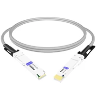
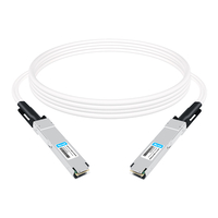
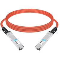
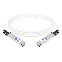
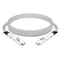
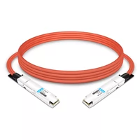
As data centers and high-performance computing environments demand faster and more reliable connectivity, OSFP DAC (Octal Small Form-factor Pluggable Direct Attach Copper) cables have emerged as a cornerstone for high-speed networking. These cables deliver exceptional bandwidth, low latency, and cost-effective solutions for short-range data transmission. In this article, we’ll explore what OSFP DAC cables are, their key features, how they compare to other technologies, practical applications, and step-by-step guidance on their use. Whether you’re a network engineer or an IT professional, this guide will help you understand why OSFP DAC is shaping the future of data center connectivity.
To better understand the design and functionality of OSFP DAC cables, it’s helpful to see them in action. The following video provides a detailed look at OSFP DAC cables, showcasing their physical characteristics and how they integrate into high-speed networking environments.
Table of Contents
ToggleWhat is OSFP DAC?
OSFP DAC cables are high-speed copper cables designed for direct connectivity between networking devices, such as switches, routers, and servers, within data centers. Utilizing the Octal Small Form-factor Pluggable (OSFP) form factor, these cables support eight differential pairs, each capable of transmitting up to 25 Gbps, resulting in a total bandwidth of 400 Gbps. Unlike optical transceivers, OSFP DAC cables use copper conductors, eliminating the need for additional optical components, which reduces costs and simplifies deployment.
To provide a clearer understanding of OSFP DAC cables, the following video offers a visual introduction to their design and functionality in high-speed networking environments.
This demonstration highlights the physical structure of OSFP DAC cables and their role in modern data centers, making it easier to grasp their practical applications.
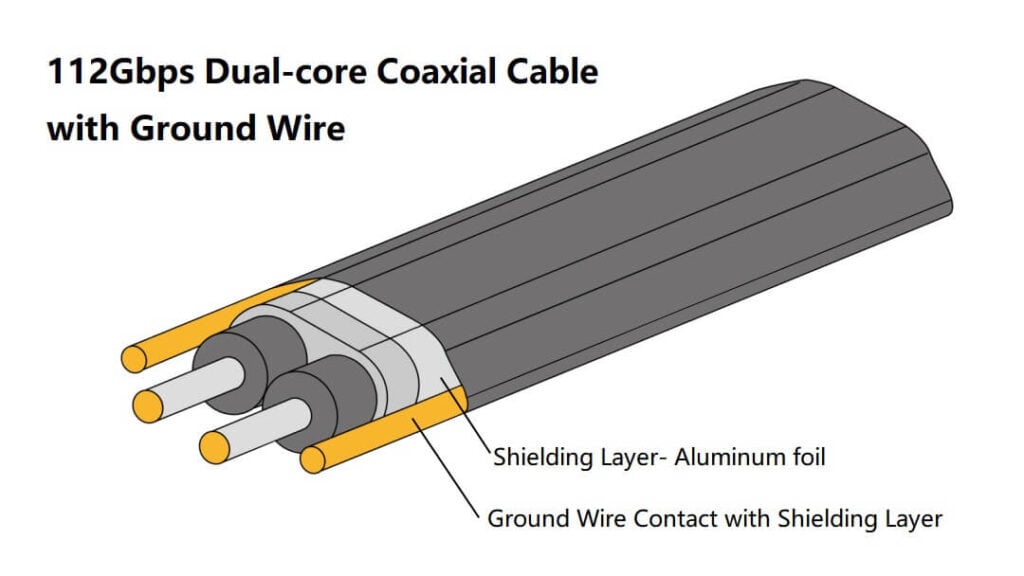
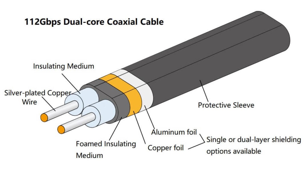
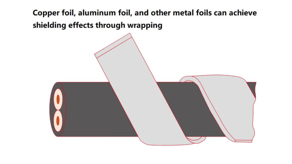
These are dual-core copper cables, which may or may not include signal return GND wires. Some cables utilize shielding metal foil connected to GND for signal return instead of GND conductors.
Key Features of OSFP DAC Cables
OSFP DAC cables are engineered to meet the demands of modern networking with the following standout features:
- High Bandwidth Capacity: With eight lanes supporting 25 Gbps each, OSFP DAC cables deliver up to 400 Gbps, ideal for bandwidth-intensive applications like AI, cloud computing, and big data analytics.
- Short-Reach Efficiency: Optimized for distances of 0.5 to 2 meters, OSFP DAC cables are perfect for intra-rack and inter-rack connections in compact data center environments.
- Low Latency: High-quality copper conductors and optimized cable designs minimize signal loss, ensuring low-latency transmission critical for real-time applications.
- Cost-Effectiveness: By eliminating the need for optical transceivers, OSFP DAC cables reduce both equipment and operational costs.
- Compatibility: Designed to connect directly to OSFP ports, these cables are compatible with a wide range of networking equipment, including NVIDIA ConnectX-7 NICs and switches from leading brands.
- Robust Design: Built with durable materials, OSFP DAC cables withstand the temperature fluctuations and physical demands of data center environments.
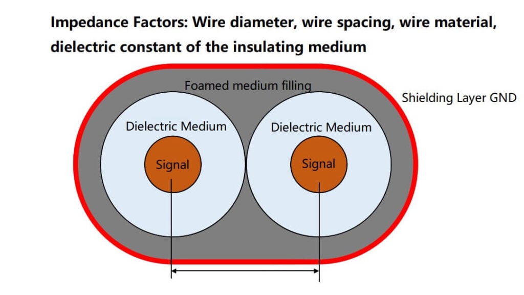
For high-frequency signals, maintaining impedance continuity is crucial. This parameter is influenced by the material of the conductor, wire diameter, spacing between wires, and the dielectric constant of the insulating medium.
Manufacturing cables to meet these stringent requirements is challenging. For instance, fluorine-containing insulating materials like Teflon, which become soft when foamed, can cause structural deformations during application, leading to impedance changes and signal distortion.
Additionally, different hardness levels of insulating medium fillings need to be considered for balance characteristics. The wave velocity of the signal correlates with the dielectric constant, and an imbalance in the dielectric constant of differential signals can lead to common-mode noise caused by delays, thereby degrading signal quality.
High-frequency signal cables are difficult to manufacture, and assembling these cables also requires consideration of solder joint impedance mismatches, wire terminal tail effects, etc.
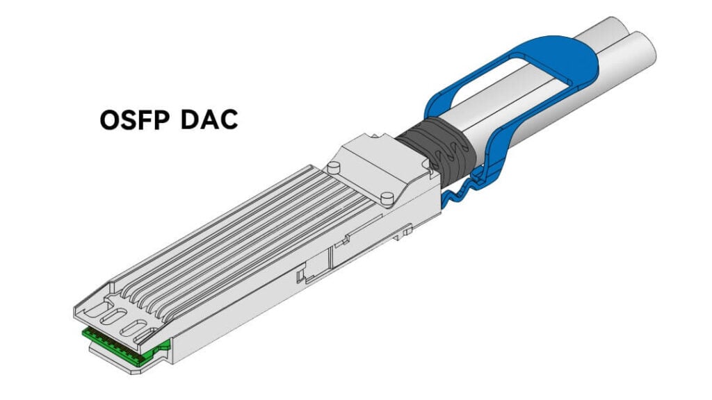
Here is an example of a FiberMall DAC with OSFP housing, commonly seen in optical modules.
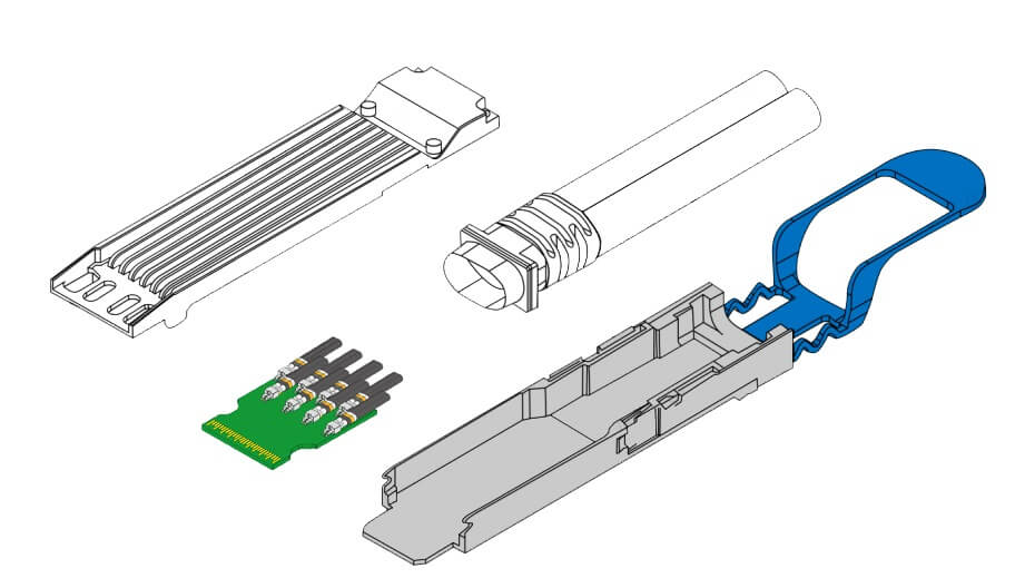
Internally, DACs are simple, with few electronic chips. One would first inspect the outer shell and the internal PCB hot-swap golden fingers, along with the cable soldering points.
OSFP DAC vs. AOC Cables
When choosing between OSFP DAC and Active Optical Cables (AOC), several factors come into play:
- Cost: OSFP DAC cables are significantly more affordable than AOC cables, as they don’t require active optical components, making them a budget-friendly choice for short-distance connections.
- Power Consumption: OSFP DAC cables, especially passive models, consume nearly zero power, compared to AOCs, which require power for active components (approximately 440mW).
- Distance: OSFP DAC cables are ideal for short reaches (0.5–2 meters), while AOCs support longer distances (up to 100 meters), making them suitable for larger data center layouts.
- Use Case: OSFP DAC excels in high-density, short-range environments like intra-rack connections, while AOCs are better for inter-rack or cross-data-center links.
The differences between OSFP DAC and AOC cables can be better appreciated through real-world demonstrations. The video below explores these technologies in action, highlighting their practical applications and performance characteristics in high-speed data center environments.
This visual comparison helps clarify when to choose OSFP DAC over AOC for your networking needs.
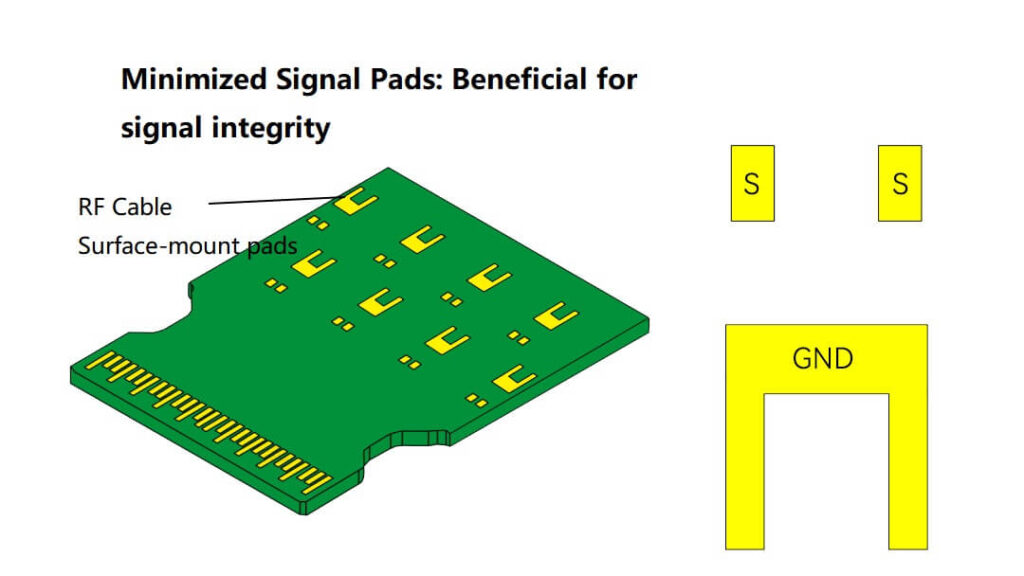
The PCB solder joints must be as small as possible to avoid resonance caused by parasitic parameters L, C, and R. FiberMall uses surface mount pads to ensure signal integrity after assembly.
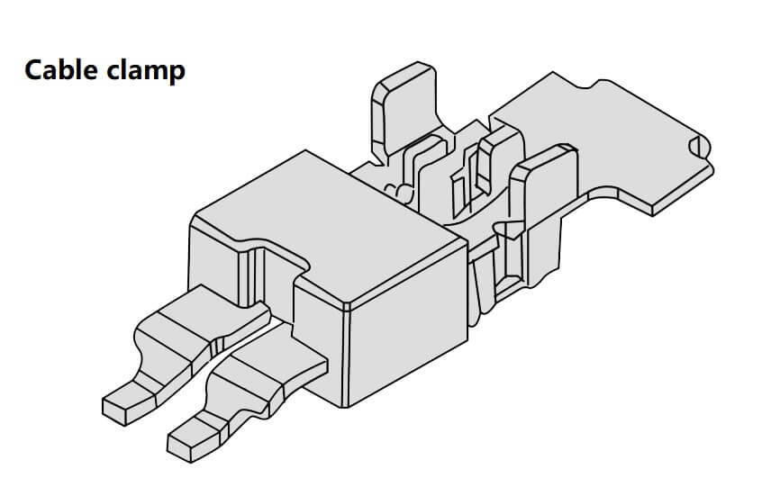
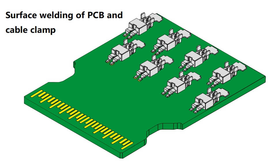
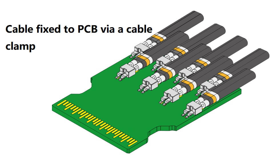
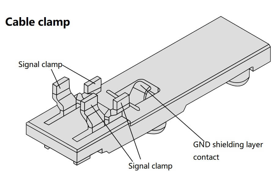
Additionally, the PCB includes a cable clamp; the clamp and PCB are soldered traditionally, while the cable and clamp are joined using laser welding to avoid distortion.
The PCB’s top surface contains 8 pairs of differential cable clamps, with another 8 pairs on the bottom.

Technical Specifications of OSFP DAC Cables
To fully appreciate the capabilities of OSFP DAC cables, understanding their technical specifications is essential:
- Data Rate: Supports up to 400 Gbps (8 lanes x 25 Gbps) using PAM4 modulation, with emerging 800G twin-port configurations available for next-generation networks.
- Cable Length: Typically ranges from 0.5 to 7 meters, with passive DACs optimized for shorter distances (0.5–2 meters) and active copper cables (ACC) extending up to 7 meters.
- Connector Type: OSFP to OSFP or OSFP to QSFP-DD configurations, with flat-top or finned-top designs for enhanced thermal management.
- Impedance Control: Designed to maintain impedance continuity, minimizing signal distortion and ensuring reliable high-frequency performance.
- Standards Compliance: Adheres to industry standards like SFF-8431 and IEEE 802.3bs, ensuring interoperability with major networking equipment brands.
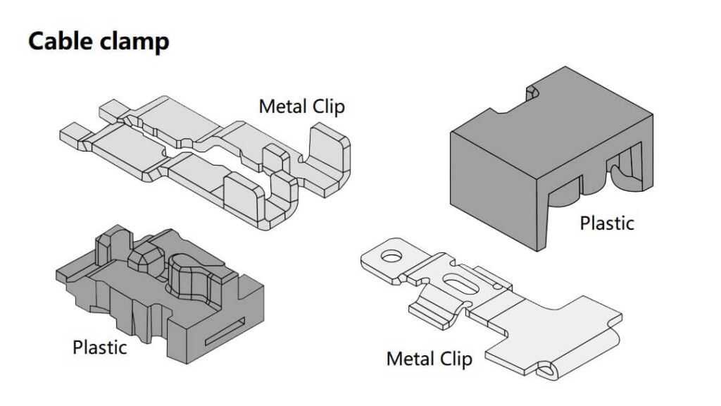
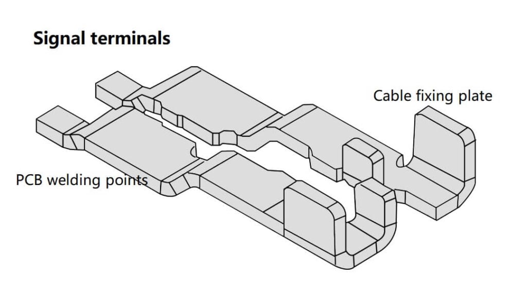
Upon dismantling the cable clamp, the internal structure reveals the signal line terminals.
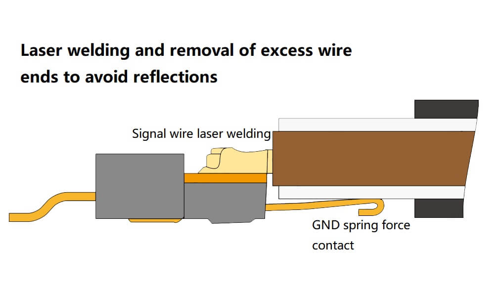
The rear end features two U-shaped slots to secure the wire cores, which are then fixed by pressing two metal pieces and laser welding.
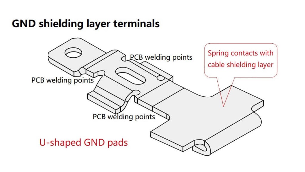
Moreover, a metal piece is used for GND connection; the front end is soldered to the PCB, and the rear end uses a spring piece for elastic contact with the cable shield layer, forming a complete signal return path.
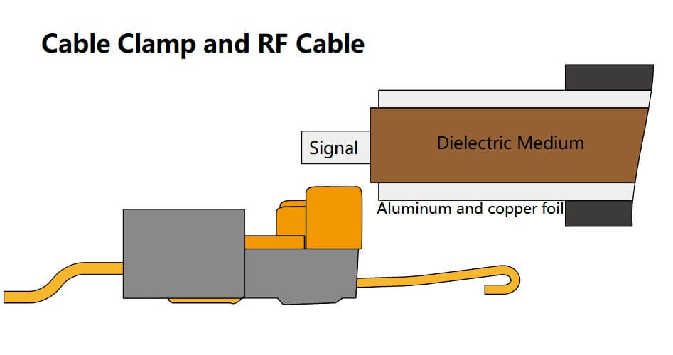
A side view shows the cable aligning and pressing into the cable clamp.
How to Install and Use OSFP DAC Cables
Deploying OSFP DAC cables in your data center is straightforward, but proper installation ensures optimal performance. Follow these steps:
- Preparation: Verify compatibility between your devices’ OSFP ports and the OSFP DAC cable. Ensure you have the correct cable length (e.g., 0.5m, 1m, or 2m) for your setup.
- Connection: Insert the OSFP DAC connector into the OSFP port of your switch, router, or server until it clicks securely. Avoid excessive force to prevent damage.
- Cable Management: Route the cable to avoid sharp bends or tension, which can affect signal integrity. Use cable organizers to optimize airflow and reduce clutter.
- Testing: Use a network tester to confirm connectivity and check for signal loss or errors. Ensure the cable meets the required bandwidth (e.g., 400 Gbps).
- Maintenance: Periodically inspect connectors for dust or damage and clean with optical-grade wipes to maintain performance.
For a step-by-step visual guide on installing OSFP DAC cables, watch the following video, which demonstrates best practices for setup and maintenance.
This tutorial provides practical tips for deploying OSFP DAC cables, ensuring seamless integration into your network.
Laser welding the signal lines ensures metallurgical bonding and removes excess terminals, avoiding noise from electromagnetic wave reflections caused by tail stub effects.
Cable clamps can come in various types.
Applications of OSFP DAC
OSFP DAC cables are widely used in high-performance environments, including:
- Data Centers: Connecting switches and servers within racks for high-speed, low-latency data transfer.
- High-Performance Computing (HPC): Supporting AI, machine learning, and scientific simulations with massive bandwidth requirements.
- Cloud Computing: Enabling fast interconnects for cloud service providers like AWS, Google Cloud, and Azure.
- InfiniBand Networks: Powering NVIDIA’s ConnectX-7 NICs and Quantum-2 switches for 400G and 800G NDR applications.
As demand for OSFP DAC grows, these cables are becoming essential for scalable, high-density networking solutions.
Industry Trends and Future of OSFP DAC
The rise of OSFP DAC cables aligns with broader industry trends toward higher bandwidth and energy efficiency. Key developments include:
- Transition to 800G: Emerging OSFP DAC solutions, like FiberMall’s 800G twin-port OSFP cables, support 2x400G configurations, catering to hyperscale data centers.
- Silicon Photonics Integration: Advances in silicon photonics are enhancing OSFP DAC performance, enabling higher baud rates and improved signal integrity.
- Sustainability: OSFP DAC cables’ low power consumption (near zero for passive models) supports eco-friendly data center designs.
- Standardization: Industry groups like the OSFP MSA ensure interoperability, driving adoption across vendors like NVIDIA, Cisco, and Arista.
Looking ahead, OSFP DAC cables are poised to support 1.6T connectivity with OSFP-XD configurations, further revolutionizing high-speed networking.
OSFP DAC cables are a game-changer for high-speed, short-range connectivity in data centers and HPC environments. With their high bandwidth, low latency, and cost-effectiveness, they meet the demands of modern applications while offering scalability for future upgrades. By understanding their features, installation best practices, and industry trends, you can leverage OSFP DAC to optimize your network infrastructure. Explore FiberMall’s full range of OSFP DAC cables to find the perfect solution for your connectivity needs.
Related Products:
-
 QDD-OSFP-FLT-PC50CM 0.5m (1.6ft) 400G QSFP-DD to OSFP Flat Top PAM4 Passive Direct Attached Cable
$154.00
-
 OSFP-FLT-400G-PC50CM 0.5m (1.6ft) 400G NDR OSFP to OSFP PAM4 Passive Direct Attached Cable, Flat top on one end and Flat top on other
$110.00
-
 OSFP-FLT-800G-AC3M 3m (10ft) 800G Twin-port 2x400G OSFP to 2x400G OSFP InfiniBand NDR Active Copper Cable, Flat top on one end and Flat top on the other
$600.00
-
 OSFP-FLT-800G-PC2M 2m (7ft) 2x400G OSFP to 2x400G OSFP PAM4 InfiniBand NDR Passive Direct Attached Cable, Flat top on one end and Flat top on the other
$300.00
-
 OSFP-800G-PC50CM 0.5m (1.6ft) 800G Twin-port 2x400G OSFP to 2x400G OSFP InfiniBand NDR Passive Direct Attach Copper Cable
$105.00
-
 OSFP-800G-AC3M 3m (10ft) 800G Twin-port 2x400G OSFP to 2x400G OSFP InfiniBand NDR Active Copper Cable
$600.00
Related posts:
- The Ultimate Guide to Direct Attach Copper Twinax Cables
- Exploring 400G QSFP-DD AOC: Understanding Active Optical Cables and Their Applications in Data Centers
- Everything You Need to Know About Arista Networks’ Compatible Cable Solutions
- The Ultimate Guide to Mellanox DAC Cable: Everything You Need to Know About Direct Attach Copper

