The recent launch of Intel’s Gaudi-3, which utilizes RoCE for Scale-UP interconnection, along with Jim Keller’s discussions on replacing NVLink with Ethernet, has brought attention to this innovative approach. Notably, Tenstorrent, where Jim Keller is involved, has cleverly implemented inter-chip network interconnection using Ethernet. Therefore, it’s pertinent to address the challenges and requirements for Ethernet to replace NVLink.
Replacing NVLink with Ethernet is not merely a matter of adopting a new transport protocol; it necessitates a series of modifications to the GPU architecture. Essentially, the issue is equivalent to figuring out how to hang High Bandwidth Memory (HBM) on an Ethernet network and achieve both Scale-Out and a series of communication optimizations to meet computational demands, such as In-Network Computing exemplified by SHARP. Globally, there are only a few individuals capable of addressing this multifaceted problem, and it’s clear that UltraEthernet has not fully grasped the concept.
To move forward, the following key questions must be addressed:
- Latency Boundary: What is the acceptable latency boundary? The link latency caused by high-throughput, high-speed SerDes FEC, and interconnection beyond the scale of tens of thousands of cards is inevitable. These issues cannot be resolved simply by modifying a packet protocol or introducing HPC-Ethernet.
- Transmission Semantics: What are the semantics of the transmission? Network professionals typically understand basic SEND/RECV operations. For instance, UEC’s definition of Reliable Unordered Delivery for Idempotent operations (RUDI) is a technical misstep. While it satisfies the commutative and idempotent laws, it fails to address how certain operations, like the idempotence of reduction addition, can be implemented. Moreover, optimizations based on the associative law, which are unsupported for the fine-grained memory access on NVLink, are also necessary. More broadly, the semantics must evolve to that of a Semi-Lattice.
- Pooling Larger Memory on NVLink: How to address the pooling of larger memory on NVLink? This involves resolving the time/space trade-offs for Compute Bound operators in computational problems, such as KV Cache.
- Dynamic Routing and Congestion Control: The ability to dynamically route and control congestion in a 1:1 non-converging Lossless network is not a significant issue for clusters with tens of thousands of cards through hardcoded tuning. However, for clusters at the scale of hundreds of thousands to millions of cards, which may even require RDMA for long-distance transmission, no commercial vendor has yet solved these problems.
Overview of Current ScaleUP Interconnection Solutions
Intel Gaudi3
According to the Gaudi3 whitepaper, the Gaudi Die is structured as follows: It incorporates 24 RoCE 200Gbps links, 21 of which are used for internal FullMesh and three for external connections.
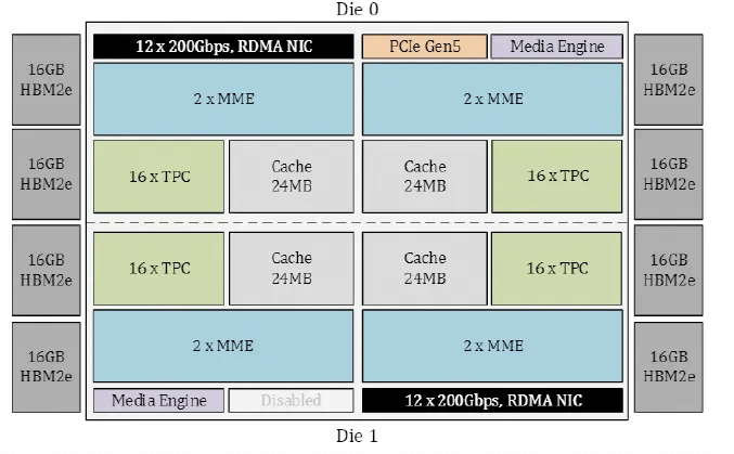
The topology for ultra-large-scale networking has been calculated, and the bandwidth of the Leaf switch is equivalent to a 25.6T switch.
Congestion Control
Intel’s whitepaper states that instead of using PFC, a Selective ACK mechanism is employed. Additionally, the SWIFT algorithm is used for Congestion Control (CC) to avoid using ECN. Essentially, this is a repurposing of Google Falcon’s Reliable Transport Engine on Intel’s IPU.
Multipath and In-Network Reduction
Intel claims to support Packet Spraying, but it is unclear which company’s switch is being used; it is certainly not their own Tofino. Therefore, it must be Broadcom. Moreover, In-Network Reduction supports FP8/BF16, etc., with Operators only supporting Sum/Min/Max. Combined with UEC’s workgroups on In-Network-Computing (INC), the picture becomes clearer.
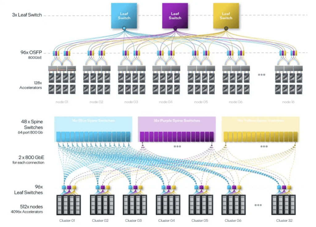
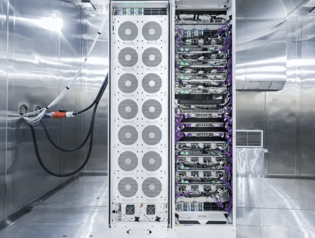
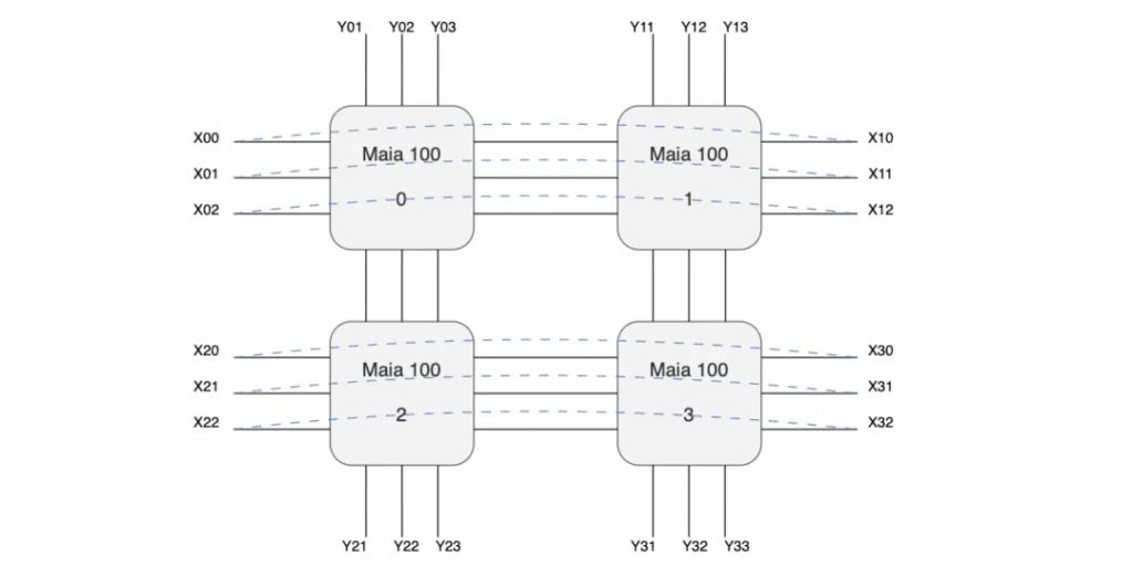
Microsoft Maia100
Limited information is available, but there is a single-chip bandwidth of 4800Gbps. A single server chassis contains four Maia100 cards and an entire cabinet with eight servers forms a cluster of 32 cards.
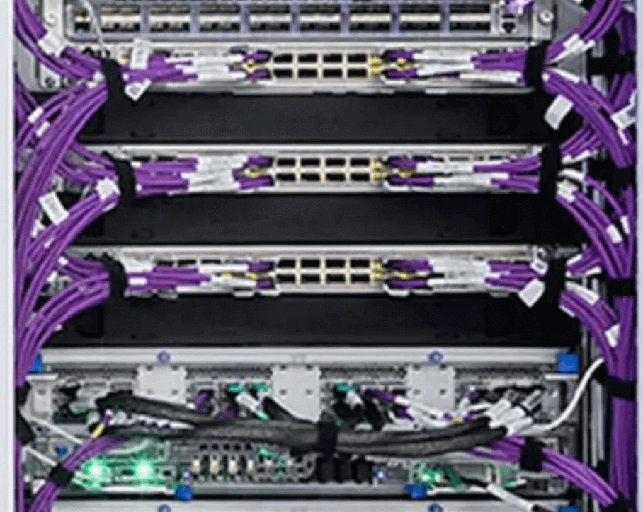
Examining the enlarged switches and interconnecting cables, there are three switches, each server having 24 400Gbps network interfaces. There are loopback connections between the ports (indicated in black in the diagram) and external interconnection lines (indicated in purple).
This suggests a topology that forms a mouth-shaped interconnection within the motherboard, creating a ring in the X direction and connecting to three switches in three planes in the Y direction.
The switches’ uplinks perform Scale-Out connections between cabinets, with each plane in each cabinet having a total of 32 400G interfaces. Adding a 1:1 convergence, the uplink switch links together to form a 25.6T switch, making a multi-layer expansion theoretically feasible. This represents a merger of Scale-Up and Scale-Out networks. As for the protocol, simple point-to-point RoCE should not pose a problem for the Torus Ring. However, multipath capabilities will be needed when interconnecting to Scale-Out switches.
The downside is the potential for higher latency. However, for custom chips that do not follow the SIMT model like CUDA but instead use a systolic array approach, latency is not a significant issue. Additionally, with only four Torus groups, the impact of collective communication latency is minimal. Personally, I believe these chips are likely used primarily for inference, as CSPs typically develop an inference chip before training chips. Other CSPs also have a clear distinction between training and inference, such as AWS Trainium/Inferentia and Google’s V5p/V5e.
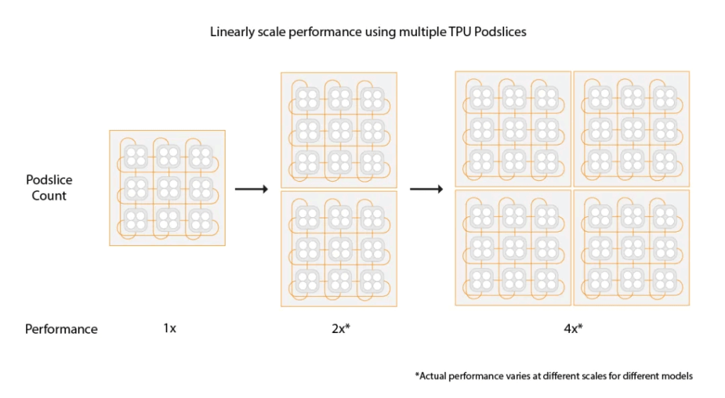
Google TPU
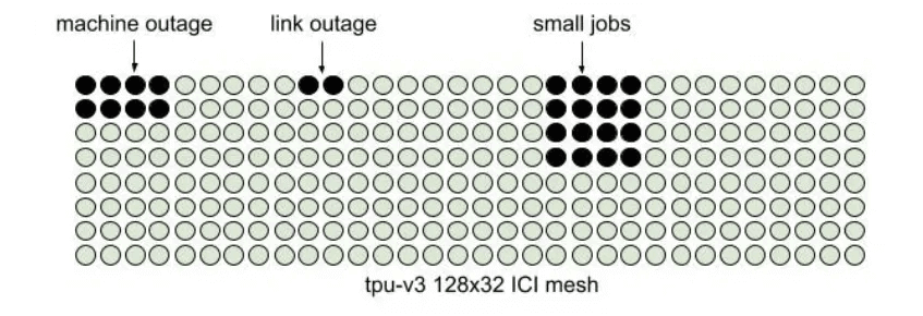
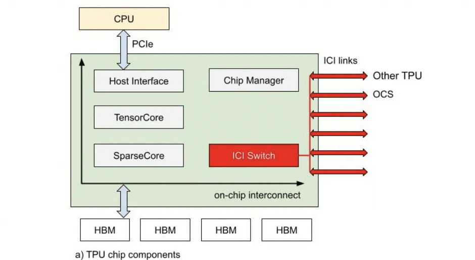
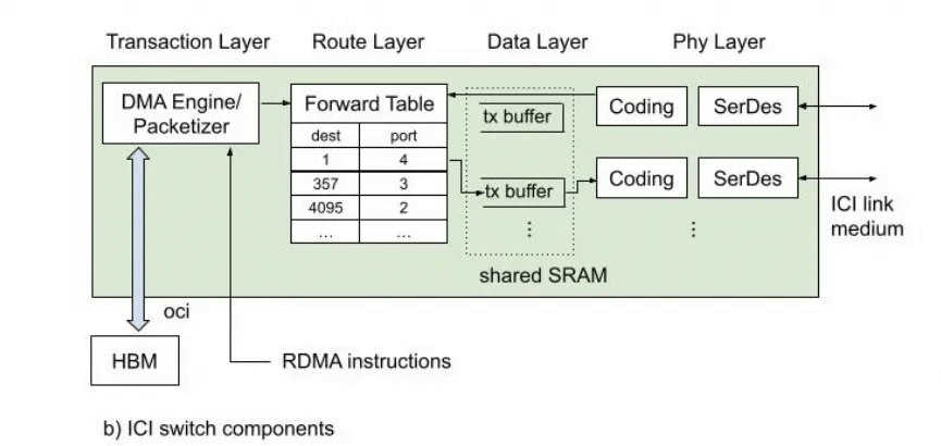
The Google TPU interconnect is well-understood, featuring a Torus Ring topology and optical switches for link switching.
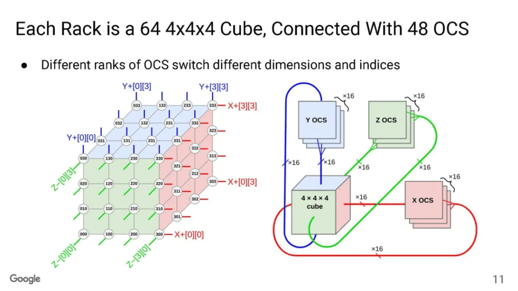
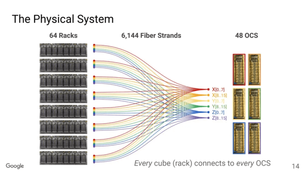
The Optical Circuit Switching (OCS) serves two purposes: dynamic partitioning according to the scale of sales, and optimization of bisection bandwidth for All-to-All communications like MoE.
For instance, a single TPUv5p chip supports a 4800Gbps Inter-Chip Interconnect (ICI) connection with a 3D-Torus topology. A cluster of 8960 TPUv5p units can be dynamically partitioned by OCS to sell different scales, with the maximum saleable configuration being 6144 units forming a 3D-Torus.
Fault tolerance is a critical consideration for the 3D Torus topology.
Additionally, Google supports extending two Pods through the data center network to build Multislice training, with Data Parallel (DP) parallelism between Pods.
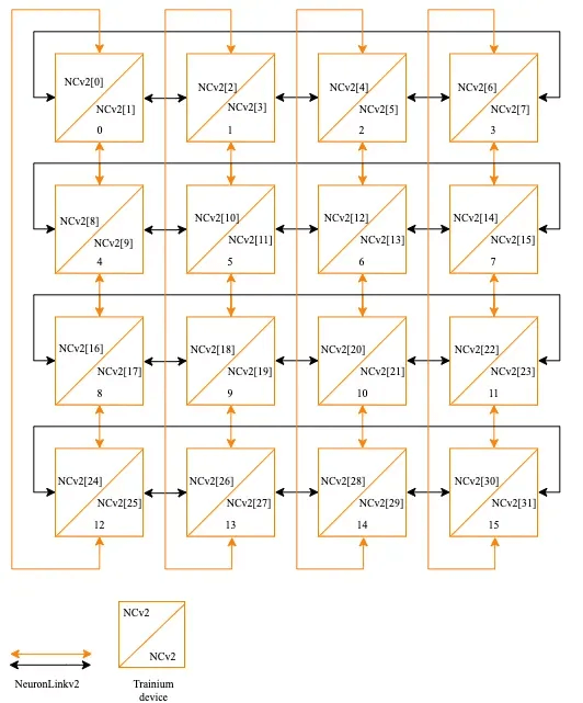
AWS Trainium
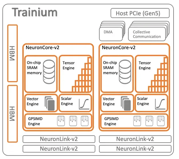
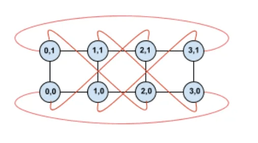
The AWS Trainium architecture consists of 16 chips forming a small cluster interconnected in a 2D Torus Ring structure.
Tesla Dojo
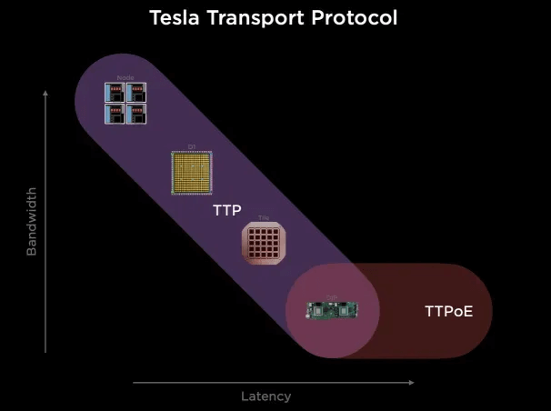
Tesla Dojo has developed its own Tesla Transport Protocol to unify Wafer/NOC and external Ethernet extensions.
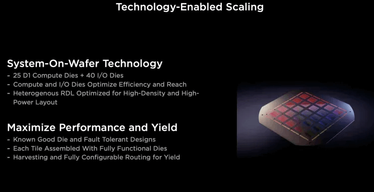
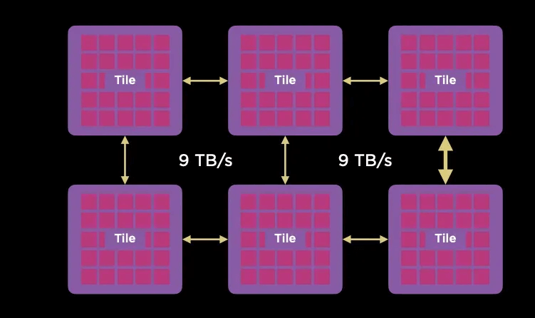
Utilizing TSMC’s System-on-Wafer, 25 D1 compute units are encapsulated on a single wafer, interconnected in a 5×5 2D Mesh network, with each wafer forming a Tile containing 40 I/O Dies.
The Tiles are interconnected at a rate of 9TB/s.
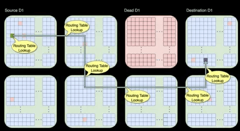
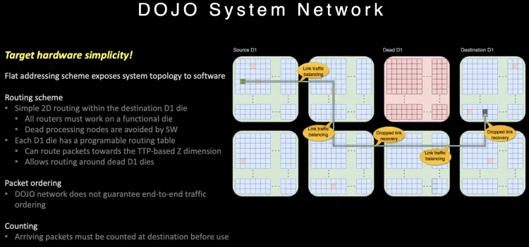
The on-chip network routing can bypass failed D1 cores or Tiles.
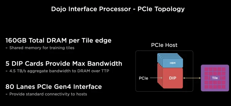
For external Scale-Out Ethernet, there is a Dojo Interface Processor (DIP) card, with each D1 compute engine having its own SRAM, and other memory placed on the HBM-equipped DIP card.
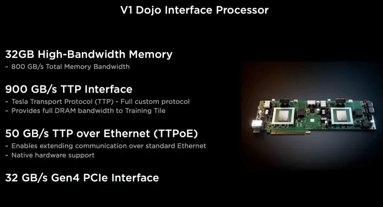
Each network card is connected to the Dojo’s I/O Die via a 900GB/s special bus, the Tesla Transport Protocol (TTP), corresponding to the 800GB HBM bandwidth, with each I/O Die able to connect to five DIP cards.
Due to the 2D Mesh network’s internal communication, long-distance communication is costly, so special routing designs have been implemented.
The routing provides multiple paths on-chip and is out-of-order. For large-scale, long-path communications, a clever use of the Dojo interface card constructs a 400Gbps Ethernet TTPoE bus as a shortcut.
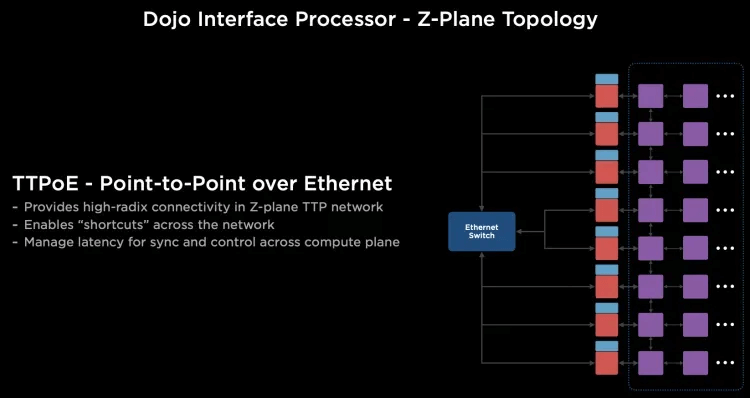
Dojo builds a high-density wafer-scale on-chip network through System-on-Wafer, and a private high-speed short-distance inter-wafer communication network at 9TB/s. I/O and memory are integrated on the DIP card, providing 900GB/s per card connected to the wafer-scale network, forming a large-scale 2D Mesh network. However, considering the congestion control due to the long communication distance on the on-chip network, a 400Gbps escape channel based on the DIP card has been designed, which sends the communication through an external Ethernet switch to the destination wafer.
Tenstorrent
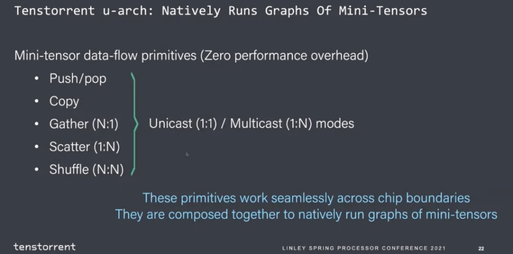
In the chip-to-chip interconnect design at Tenstorrent, Jim Keller utilized Ethernet, which has a simple structure. The Tensor + control header forms an Ethernet packet and can trigger conditional execution capabilities, as shown below:
Full chip-to-chip interconnect using Ethernet
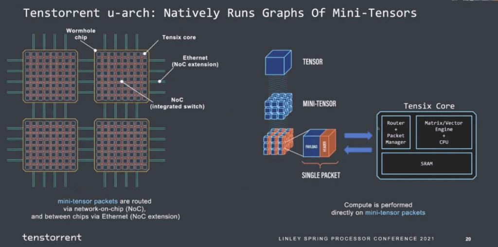
Supports multiple functional communication source languages
Then there is the partitioning of the graph. It seems that the number of instructions per stage can be estimated, and the bandwidth of operators entering and leaving can also be estimated.
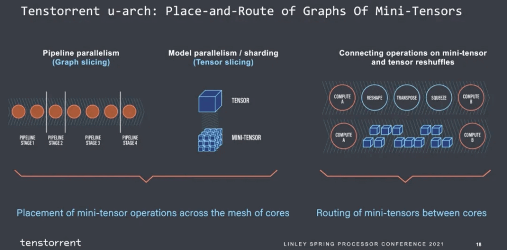
The final mapping constraints to the cores also appear to be straightforward:
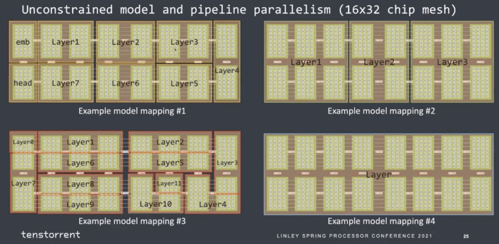
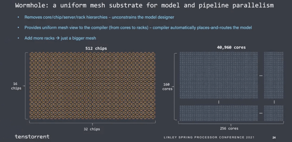
A simple 2D mesh structure
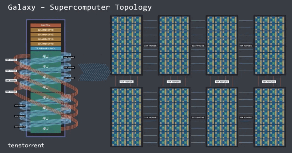
Can be scaled up to 40,960 cores for large-scale interconnects
Technical Requirements for Scale-UP
Topology Selection
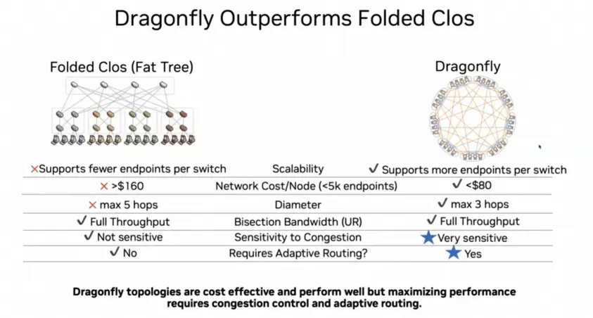
In the ScaleUp network topology selection, we can observe that Nvidia currently uses a 1:1 converging Fat Tree structure, while other companies mostly use Torus Ring or 2D Mesh topologies. Nvidia will later evolve to DragonFly.
The logic behind this choice can be seen in the hammingMesh paper:
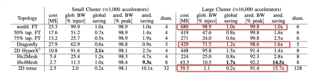
For Allreduce bandwidth, Torus is the most cost-effective and can basically reach peak performance. However, for models like MoE that require AlltoAll, the bisection bandwidth needs to be considered. DragonFly performs well in terms of wiring complexity, global bandwidth, and network diameter.
Dynamic Routing and Reliable Transmission
While everyone is criticizing the shortcomings of RoCE, the fact is that BF3+Spectrum-4 has Adaptive Routing, Broadcom has DLB/GLB to evolve Packet Spraying, and there are also VoQ technologies similar to Cisco’s. Meta also has multi-path static routing for traffic engineering or affinity scheduling in the control plane.
However, these solutions can only solve part of the problems at the scale of tens of thousands of cards. The real challenge comes when scaling to hundreds of thousands of cards. How do we address this?
Algorithmically solving burst is a difficult task, and even more challenging is that no one is trying to understand the root cause of bursts. Instead, they are constantly trying to test switch buffers to mitigate bursts, and some are even exploring deterministic networking and Fourier analysis. This is simply missing the point.
This is a very difficult problem, and it remains to be seen when the other industry players will figure it out. Another aspect is system failure and elastic scaling. Google’s NSDI24 paper mentions the reasons for fragmentation.
If these issues are not considered, it will lead to scheduling challenges. A good choice could be the implementation of the routing table within ICI, coupled with OCS switches.
Why is this important for Ethernet to support ScaleUP? Because Ethernet needs to implement a routing layer here to support DragonFly and failed link switching capabilities.
Is Latency Important for Scale UP?
The essence of this question is how GPUs perform Latency Hiding, and the differences in latency between NVLink and RDMA. It’s important to note that GPUs are inherently Throughput Optimized processors, and if they were to pursue low latency, it would indicate issues with their implementation. The fundamental problem is that NVLink uses memory semantics, while RDMA uses message semantics, and there are also challenges in implementing RDMA for heterogeneous computing.
Shortcomings of RDMA Implementation
The key factor causing higher latency in RDMA compared to NVLink is the CPU.
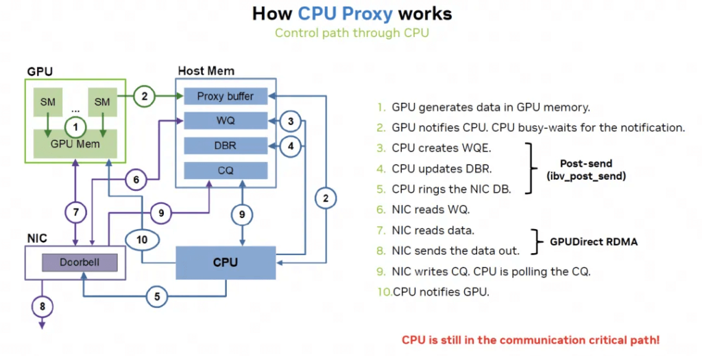
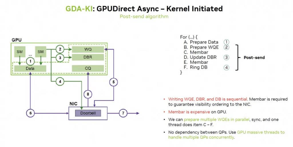
Nvidia is addressing this through GDA-KI, which helps hide many memory access latencies more effectively.
Fine-Grained Memory Access
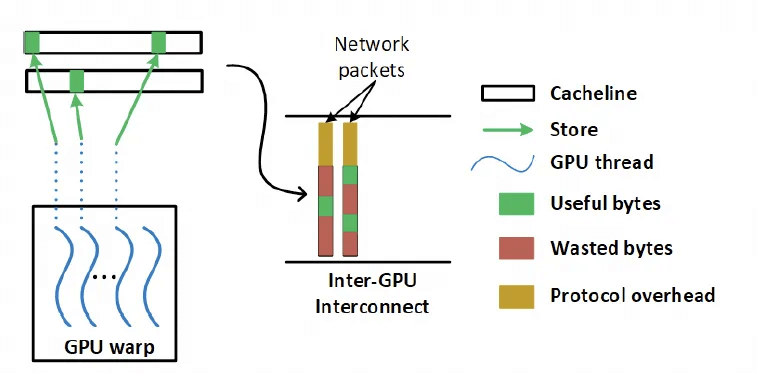
Another issue is that NVLink is based on memory semantics and has a large number of fine-grained Load/Store accesses, making transmission efficiency and latency very important. But how can this be done using Ethernet RDMA? It would require HPC Ethernet, as the packets would be too large.
This is the problem I’ve been discussing in NetDAM – the need for a Semi-Lattice semantic for RDMA messages:
- Commutativity ensures data can be submitted in an unordered manner.
- Idempotence solves the ambiguity problem of dropped packets and retransmissions, but for operations like Reduce with side effects, transaction-based or data idempotence is required.
- Associativity helps improve transmission efficiency for fine-grained memory accesses through scheduling.
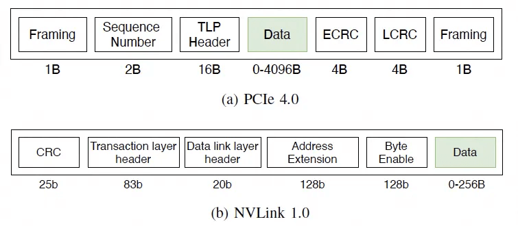
For memory access requirements, the in-host protocol is typically FLIT-sized. To support this while also enabling ultra-scale ScaleUP interconnects, reliability, routing headers, Ethernet headers, multi-tenant isolation (VPC headers), etc., the key is to leverage associativity. However, UEC seems to have completely missed this, only providing support for commutativity and idempotence in RUDI.
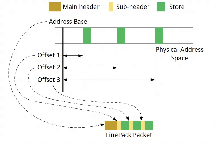
Nvidia’s solution is associativity encoding, which solves the fine-grained access problem.
The next generation of NVLink will likely converge with Infiniband, and ScaleOut and ScaleUP networks will eventually merge.
Memory Pooling for ScaleUP
Many large models today suffer from the limited capacity of HBM (High-Bandwidth Memory). While NVIDIA has addressed this by connecting Grace and NVLink C2C to extend the memory, the fundamental issue is that ScaleUP networking requires memory pooling.
Conclusions
- Any company aiming to do Ethernet ScaleUP needs to consider the following key challenges:
- Latency is not as critical. By modifying GPU memory access patterns to align with message semantics and then caching the processing, the latency can be hidden.
- The dynamic routing and tenant isolation capabilities of the ScaleUP network are crucial. Effective routing solutions are needed, especially to address the fragmentation issues caused by link failures.
- RDMA (Remote Direct Memory Access) semantics are imperfect, and simply copying SHARP (Scalable Hierarchical Aggregation and Reduction Protocol) has many pitfalls. A Semi-Lattice semantic is required, supporting a series of side-effect operations to achieve idempotence.
- Fabric multipath forwarding and congestion control are needed to improve overall fabric utilization.
- Large-scale memory pooling is essential.
Related Products:
-
 NVIDIA MMS4X00-NM-FLT Compatible 800G Twin-port OSFP 2x400G Flat Top PAM4 1310nm 500m DOM Dual MTP/MPO-12 SMF Optical Transceiver Module
$1199.00
NVIDIA MMS4X00-NM-FLT Compatible 800G Twin-port OSFP 2x400G Flat Top PAM4 1310nm 500m DOM Dual MTP/MPO-12 SMF Optical Transceiver Module
$1199.00
-
NVIDIA MMA4Z00-NS-FLT Compatible 800Gb/s Twin-port OSFP 2x400G SR8 PAM4 850nm 100m DOM Dual MPO-12 MMF Optical Transceiver Module
$650.00
-
NVIDIA MMS4X00-NM Compatible 800Gb/s Twin-port OSFP 2x400G PAM4 1310nm 500m DOM Dual MTP/MPO-12 SMF Optical Transceiver Module
$900.00
-
NVIDIA MMA4Z00-NS Compatible 800Gb/s Twin-port OSFP 2x400G SR8 PAM4 850nm 100m DOM Dual MPO-12 MMF Optical Transceiver Module
$650.00
-
NVIDIA MCA4J80-N003-FLT Compatible 3m (10ft) 800G Twin-port 2x400G OSFP to 2x400G OSFP InfiniBand NDR Active Copper Cable, Flat top on one end and Flat top on the other
$600.00
-
NVIDIA MCP7Y10-N001 Compatible 1m (3ft) 800G InfiniBand NDR Twin-port OSFP to 2x400G QSFP112 Breakout DAC
$155.00
-
NVIDIA MMS1Z00-NS400 Compatible 400G NDR QSFP112 DR4 PAM4 1310nm 500m MPO-12 with FEC Optical Transceiver Module
$700.00
-
NVIDIA MMS4X00-NS400 Compatible 400G OSFP DR4 Flat Top PAM4 1310nm MTP/MPO-12 500m SMF FEC Optical Transceiver Module
$700.00
-
NVIDIA MMA1Z00-NS400 Compatible 400G QSFP112 VR4 PAM4 850nm 50m MTP/MPO-12 OM4 FEC Optical Transceiver Module
$550.00
-
NVIDIA MMA4Z00-NS400 Compatible 400G OSFP SR4 Flat Top PAM4 850nm 30m on OM3/50m on OM4 MTP/MPO-12 Multimode FEC Optical Transceiver Module
$550.00
-
NVIDIA MFP7E10-N003 Compatible 3m (10ft) 8 Fibers Low Insertion Loss Female to Female MPO Trunk Cable Polarity B APC to APC LSZH Multimode OM3 50/125
$35.00
-
NVIDIA MFP7E30-N003 Compatible 3m (10ft) 8 Fibers Low Insertion Loss Female to Female MPO Trunk Cable Polarity B APC to APC LSZH Single-Mode OS2 9/125
$42.00