
DeepSeek has led to an explosion in demand for inference, and a hole has been torn in Nvidia’s “computing power hegemony”. The door to a new world has gradually opened—the computing power revolution led by ASIC chips is moving from silence to noise.
Recently, Core Flow Think Tank quoted an informed source as saying that DeepSeek is preparing to develop its own AI chips. Compared with this up-and-coming company, domestic giants such as Alibaba, Baidu, and ByteDance have already crossed the door of “self-research” earlier.
On the other side of the ocean, new progress in OpenAI’s self-developed chips was also released at the beginning of the year. Foreign media revealed that the first chip customized by Broadcom for it will be produced at TSMC within a few months. It was previously reported that Sam Altman planned to raise $7 trillion to build a “chip empire” covering both design and manufacturing. In addition, Google, Amazon, Microsoft, and Meta have also joined the “self-research craze”.
One obvious signal is that no matter whether it is DeepSeek, OpenAI, Chinese companies or Silicon Valley giants, no one wants to fall behind in the era of computing power. And ASIC chips may become their ticket to enter the new world.
Will this “kill” Nvidia? Or, will it “recreate” a second Nvidia? There is no answer yet. However, it is clear that companies in upstream industry chain have already foreseen the vigor of this “self-developed wave”. For example, Broadcom, which provides design and customization services to major manufacturers, has “taken off” in performance: in 2024, AI business revenue increases by 240% year-on-year to US$3.7 billion; AI business revenue in Q1 2025 is $4.1 billion, up 77% year-on-year; 80% of them come from ASIC chip design. In Broadcom’s eyes, the ASIC chip market is worth more than $90 billion.
From GPU to ASIC, Computing Power Economics is Reaching a Watershed
Low cost is a prerequisite for the explosion of AI reasoning. In contrast, general-purpose GPU chips have become the golden shackles for the explosion of AI.
NVIDIA’s H100 and A100 are the absolute kings of large model training, and even B200 and H200 are sought after by technology giants. The Financial Times previously cited data from Omdia that in 2024, the main customers of Nvidia’s Hopper architecture chips include Microsoft, Meta, Tesla/xAI, etc., among which Microsoft’s orders will reach 500,000.
However, as the absolute ruler of general-purpose GPUs, the other side of the coin of NVIDIA’s product solutions has gradually become apparent: high costs and redundant energy consumption.
In terms of cost, a single H100 costs more than $30,000. Training a model with hundreds of billions of parameters requires tens of thousands of GPUs, plus subsequent investments in network hardware, storage, and security, totaling more than $500 million. According to HSBC data, the latest generation of GB200 NVL72 solution costs more than US$3 million per cabinet, and NVL36 is around US$1.8 million.
It can be said that model training based on general-purpose GPUs is too expensive, but Silicon Valley, with unlimited computing power, still prefers the narrative of “big power makes bricks fly”, and capital expenditures have not slowed down. Just recently, Musk’s xAI, which recently announced Grok-3, has a server scale of 200,000 GPUs for training.
The article “20,000 Words Detailed Explanation of Key AI Insights for 2025” jointly released by Tencent Technology and Silicon Rabbit Racing mentioned that hyperscale data center operators expect capital expenditures (CapEx) to exceed US$200 billion in 2024, and this figure is expected to be close to US$250 billion by 2025, and major resources will be allocated to artificial intelligence.
In terms of energy consumption, according to SemiAnalysis’s calculations, a 100,000-card H100 cluster has a total power consumption of 150MW and consumes 1.59TWh of electricity per year. Calculated at $0.078 per kilowatt-hour, the annual electricity bill is as high as $123.9 million. Compared with the data released by OpenAI, the computing power utilization rate of GPU in the inference stage is only 30%-50%, and the phenomenon of “calculating while waiting” is significant. Such inefficient performance utilization is indeed a serious waste of resources in the era of inference.
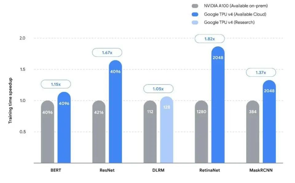
Google’s previously announced TPU V4 and A100 training speeds for different architecture models
Leading performance, high prices, poor efficiency, and ecological barriers have forced the industry to say “the world has suffered from Nvidia for a long time” over the past year—cloud vendors are gradually losing hardware autonomy, coupled with supply chain risks, and AMD is temporarily “unable to grow”. Many factors have forced the giants to start developing their own ASIC dedicated chips.
Since then, the AI chip battlefield has shifted from a technological competition to an economic game. As Southwest Securities’ research concluded, “When the model architecture enters the convergence period, every dollar invested in computing power must produce quantifiable economic benefits.” Judging from the recent progress reported by North American cloud vendors, ASIC has shown certain substitution advantages:
- Google: The TPU v5 chip customized by Broadcom for Google has a unit computing power cost that is 70% lower than that of H100 in the Llama-3 reasoning scenario.
- Amazon: AWS Trainium 3, with a 3nm process, consumes only 1/3 of the energy of a general-purpose GPU with the same computing power, saving more than 10 million US dollars in electricity costs annually; It is understood that Amazon’s Trainium chip shipments in 2024 have exceeded 500,000 pieces.
- Microsoft: According to IDC data, after Microsoft Azure developed its own ASIC, the proportion of hardware procurement costs dropped from 75% to 58%, breaking away from the long-term passive bargaining dilemma.
As the biggest beneficiary of the North American ASIC chain, Broadcom’s trend is becoming increasingly evident in the data.
Broadcom’s AI business revenue in 2024 was US$3.7 billion, a year-on-year increase of 240%, of which 80% came from ASIC design services. In Q1 2025, its AI business revenue was US$4.1 billion, a year-on-year increase of 77%. At the same time, it expects AI revenue to be US$4.4 billion in the second quarter, a year-on-year increase of 44%.
As early as during the annual report period, Broadcom guided that ASIC revenue would explode in 2027, painting a pie in the sky for the market that ASIC chips would be expected to reach a market size of US$90 billion three years later. The company reiterated this during the Q1 conference call.
With this major industry trend, Broadcom has become the world’s third semiconductor company with a market value of over $1 trillion after Nvidia and TSMC. It has also attracted overseas attention to companies such as Marvell and AIchip.
However, one thing needs to be emphasized: “ASIC is good, but it will not kill GPU.” Microsoft, Google, and Meta are all developing their own products, but at the same time they are all vying to be the first to launch Nvidia’s B200, which actually shows that there is no direct competitive relationship between the two parties.
A more objective conclusion should be that GPUs will still dominate the high-performance training market and will still be the most important chip in inference scenarios due to their versatility. However, in the future blue ocean market of AI chips approaching $400 billion, the penetration path of ASICs is already clearly visible.
IDC predicts that in the inference scenarios from 2024 to 2026, the proportion of ASIC will increase from 15% to 40%, or a maximum of US$160 billion. The end result of this transformation may be: ASIC takes over 80% of the inference market, and GPU retreats to the training and graphics fields.
The real winners will be those “dual-players” who understand both silicon wafers and scenarios. Nvidia is obviously one of them. Being optimistic about ASIC is definitely not talking down Nvidia. The guide to the new world is to find dual players other than Nvidia and how to make money in the new era of ASIC.
ASIC’s “Scalpel” Cuts off all non-core Modules
It is said that ASIC is good for AI reasoning, but what kind of chip is it?
From an architectural perspective, the limitation of general-purpose chips such as GPUs is their “one against a hundred” design—they need to take into account multiple requirements such as graphics rendering, scientific computing, and different model architectures, resulting in a large amount of transistor resources being wasted on non-core functional modules.
The biggest feature of NVIDIA GPU is that it has many “small cores”, which can be compared to the multiple engines of the Falcon rocket. Developers can rely on the operator library accumulated by CUDA over the years to call these small cores for parallel computing smoothly, efficiently and flexibly.
But if the downstream model is relatively certain, the computing task is relatively certain, and there is no need for so many small cores to maintain flexibility. This is the underlying principle of ASIC, so it is also called a fully customized high-computing power chip.
Through “scalpel-like” precise cutting, only hardware units that are strongly relevant to the target scenario are retained, unleashing amazing efficiency, which has been verified in the products of Google and Amazon.
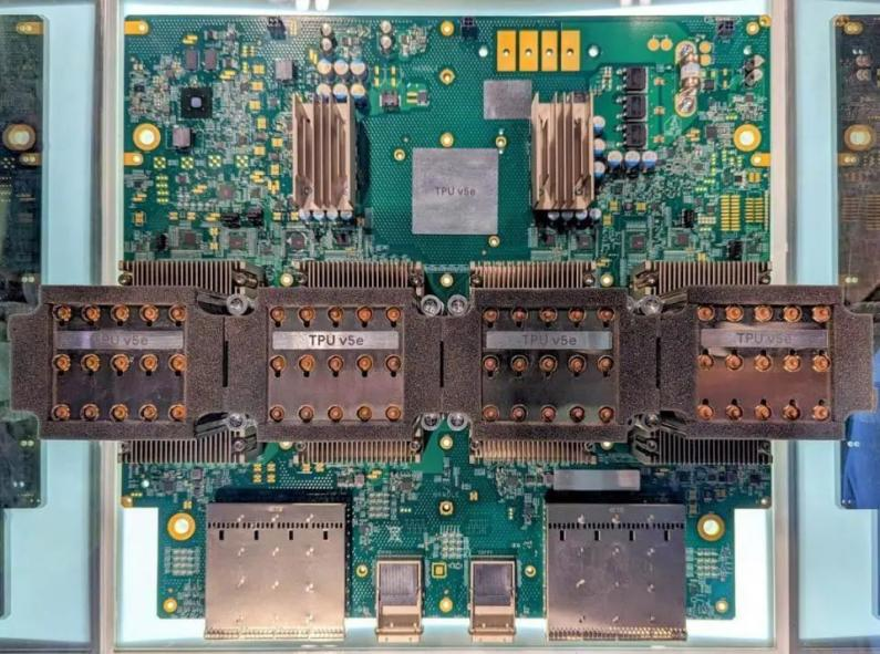
Google TPU v5e AI accelerator real shot
For GPUs, the best tool to call them is NVIDIA’s CUDA, while for ASIC chips, they are called by the algorithms developed by cloud vendors themselves. This is not a difficult task for large companies that started out as software vendors:
- In Google TPU v4, 95% of the transistor resources are used for matrix multiplication units and vector processing units, which are optimized for neural network calculations, while similar units in GPUs account for less than 60%.
- Unlike the “computing-storage” separation model of the traditional von Neumann architecture, ASIC can customize data flow around algorithm characteristics. For example, in the recommended system chip customized by Broadcom for Meta, the computing unit is directly embedded around the storage controller, shortening the data movement distance by 70% and reducing the latency to 1/8 of the GPU.
- In response to the 50%-90% sparse weight characteristics in AI models, the Amazon Trainium2 chip is embedded with a sparse computing engine that can skip the zero-value calculation link, improving theoretical performance by 300%.
When algorithms tend to be fixed, ASIC has a natural advantage for deterministic vertical scenarios. The ultimate goal of ASIC design is to make the chip itself the “physical embodiment” of the algorithm.
In past history and current reality, we can find examples of ASIC success, such as mining machine chips.
In the early days, the industry used Nvidia’s GPUs for mining. Later, as the difficulty of mining increased, electricity consumption exceeded mining revenue (very similar to the current inference needs), and dedicated ASIC chips for mining exploded. Although its versatility is far less than that of GPU, mining ASICs maximize parallelism.
For example, Bitmain’s Bitcoin mining ASIC deploys tens of thousands of SHA-256 hash computing units at the same time, achieving super-linear acceleration under a single algorithm, and the computing power density is more than 1,000 times that of GPU. Not only has the dedicated capability been greatly improved, but energy consumption has also been saved at the system level.
In addition, the use of ASIC can streamline peripheral circuits (for example, the complex protocol stack of the PCIe interface is no longer needed), reduce the mainboard area by 40%, and cut the cost of the entire machine by 25%.
Low cost, high efficiency, and support for deep integration of hardware and scenarios, these ASIC technology cores are naturally adapted to the AI industry’s transformation needs from “computational brute-forcing” to “refined efficiency revolution.”
With the advent of the inference era, ASIC cost advantages will repeat the history of mining machines and achieve a “death cross” under scale effect – despite the high initial R&D costs (the design cost of a single chip is approximately US$50 million), its marginal cost decline curve is much steeper than that of general-purpose GPUs.
Taking Google TPU v4 as an example, when the shipment volume increased from 100,000 pieces to 1 million pieces, the cost per piece dropped sharply from US$3,800 to US$1,200, a drop of nearly 70%, while the cost drop of GPU usually does not exceed 30%. According to the latest information from the industry chain, Google TPU v6 is expected to ship 1.6 million units in 2025, with the computing power of a single chip three times higher than the previous generation. The cost-effectiveness of ASIC is still increasing rapidly.
This leads to a new topic: can everyone join the trend of self-developed ASIC? This depends on the self-research cost and demand.
According to the calculation of ASIC inference accelerator card with 7nm process, the one-time tape-out costs including IP licensing fees, labor costs, design tools, mask templates, etc. may be in the hundreds of millions of yuan, not including the subsequent mass production costs. In this regard, large companies have greater financial advantages.
At present, cloud vendors such as Google and Amazon have a mature customer system, can form a closed loop of R&D and sales, and have inherent advantages in self-research.
For companies like Meta, the logic behind their self-developed business is that they already have a massive demand for computing power internally. Earlier this year, Zuckerberg revealed that he plans to launch about 1GW of computing power in 2025 and have more than 1.3 million GPUs by the end of the year.
The “New Map” is Worth Far more than $100 Billion
The demand for mining alone has brought about a market of nearly $10 billion, so when Broadcom announced that the AI ASIC market space would be $70-90 billion by the end of 2024, we were not surprised, and even thought that this number might be conservative.
Now, the industrial trend of ASIC chips should no longer be questioned, and the focus should be on how to master the rules of the game in the “new map”. In the nearly $100 billion AI ASIC market, three clear echelons have been formed: “ASIC chip designers and manufacturers who set the rules”, “industry chain supporting”, and “Fabless in vertical scenarios”.
The first tier is the ASIC chip designers and manufacturers who set the rules. They can manufacture ASIC chips with a unit price of more than $10,000 and cooperate with downstream cloud vendors for commercial use. Representative players include Broadcom, Marvell, AIchip, and TSMC, the foundry king that will benefit from any advanced chip.
The second tier is the supporting industrial chain. The supporting logic that has attracted market attention includes advanced packaging and the downstream industrial chain.
- Advanced packaging: 35% of TSMC’s CoWoS production capacity has been transferred to ASIC customers, including domestic counterparts such as SMIC, Changdian Technology, and Tongfu Microelectronics.
- The decoupling of cloud vendors and NVIDIA’s hardware solutions brings new hardware opportunities, such as AEC copper cables. Amazon’s self-developed single ASIC needs to be equipped with 3 AECs. If 7 million ASICs are shipped in 2027, the corresponding market will exceed US$5 billion. Others chances including servers and PCBs will benefit from similar logic.
The third tier is the Fabless of vertical scenarios that are in the making. The essence of ASIC is a demand-driven market. Whoever can capture the pain points of the scenario first will have the pricing power. The gene of ASIC is customization, which is naturally adapted to vertical scenarios. Take intelligent driving chips as an example. As a typical ASIC chip, with BYD and other companies going all in on intelligent driving, this type of product is beginning to enter a period of explosive growth.
The opportunities corresponding to the three major echelons of the global ASIC industry chain can be regarded as the “three secret keys” of domestic production.
Due to the restrictions of the ban, the gap between domestic GPUs and NVIDIA is still huge, and ecological construction is also a long journey. However, for ASICs, we are even on the same starting line as overseas. Combined with vertical scenarios, many Chinese Fabless companies can make more energy-efficient products, such as the aforementioned mining machine ASICs, smart driving ASICs, and Baidu’s Kunlun Core.
The supporting chip manufacturing mainly relies on SMIC, while ZTE Microelectronics, a subsidiary of ZTE, is a new entrant. It is not ruled out that they will cooperate with domestic manufacturers in the future to stage a drama of “Who will be the Chinese Broadcom?”
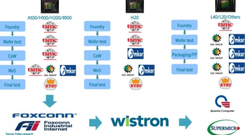
Nvidia’s main upstream suppliers of data center products
The supporting part of the industrial chain is relatively easy to produce. For the corresponding servers, optical transceivers, switches, PCBs, and copper cables, domestic companies are inherently more competitive due to their low technical difficulty. At the same time, these industry chain companies have a “symbiotic” relationship with domestic computing power, and the ASIC chip industry chain will not be absent.
In terms of application scenarios, in addition to the repeatedly mentioned intelligent driving chips and AI inference acceleration cards, the opportunities for other domestic design companies depend on which scenarios can become popular and which companies can seize the opportunities.
Conclusion
As AI leaps from the training hard work to the deep waters of reasoning in pursuit of energy efficiency, the second half of the computing power war is destined to belong to those companies that can transform technological fantasies into economic accounts.
The counterattack of ASIC chips is not only a technological revolution, but also a business revelation about efficiency, cost and voice. In this new game, the chips of Chinese players are quietly increasing – opportunities always come to those who are prepared.