800G Pluggable Optical Module
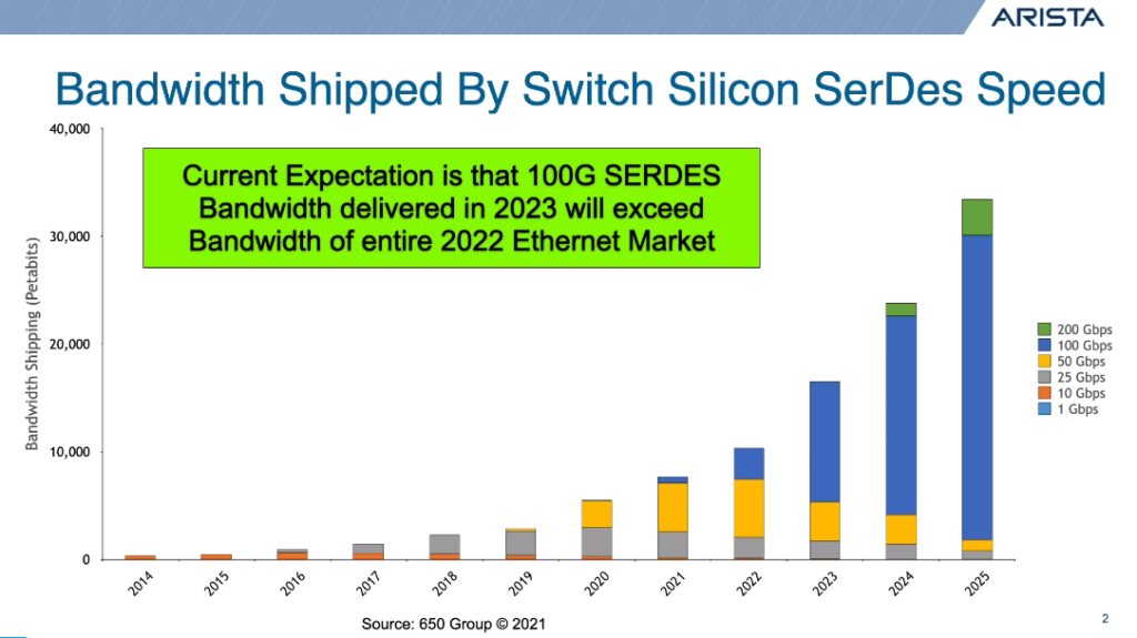
In a data center network, the performance and bandwidth of the switch chip is a very important factors, and the performance and bandwidth of the switch chip depend on its internal SerDes circuitry, which is a kind of circuitry that converts serial data to parallel data or parallel data to serial data and enables high-speed, low-power, and low-latency data communication. The mainstream SerDes on the market today have a speed of 100Gbps (100 billion bits per second), which means that each channel can transmit 100Gbps of data. This SerDes technology is referred to as 100G SerDes. according to one report, the bandwidth of switch chips using 100G SerDes is projected to exceed the bandwidth of the entire Ethernet market in 2022 by 2023, reaching 13.8 ZB (13.8 Gigabytes per year).
800G Fiber and 800G Ethernet are two emerging technologies as the need for high-speed data transmission in data center networks continues to grow. 800G Fiber is an optical device that can transmit 800Gbps of data over optical fiber. 800G Fiber can be implemented using different SerDes configurations, such as dual 400G or eight 100G. 800G Fiber has the advantage of improving network performance and efficiency, but the disadvantage of higher power consumption and cost. Currently, 800G Fiber is in its early stages and is offered by some of the leading vendors and is primarily used to interconnect hyperscale data centers.
800G Ethernet is a network standard that defines how to transmit 800Gbps of data over Ethernet. 800G Ethernet specification was finalized by the Ethernet Technology Alliance in April 2020. 800G Ethernet specification includes a variety of Physical Layer Interface (PHY) and Media Access Control Layer (MAC) parameters to accommodate different application scenarios and distance requirements. The advantage of 800G Ethernet is that it can provide higher network capacity and flexibility, but the disadvantage is that it requires more complex technology and standardization work. Currently, 800G Ethernet is still in the development stage, and commercial products are expected to start appearing in 2023. 800G optics will be ready before 800G Ethernet. The rapid growth of cloud computing has created a demand for 800G optics, especially for AI/ML applications that rely on high-performance and low-cost optics. 800G optics can provide higher bandwidth and spectral efficiency, support more complex modulation formats and algorithms, and adapt to different data center network architectures and scenarios. 800G optics also enable hybrid deployments with 400G optics for increased network flexibility and compatibility. 800G optics can also be deployed in hybrid with 400G optics for increased network flexibility and compatibility.
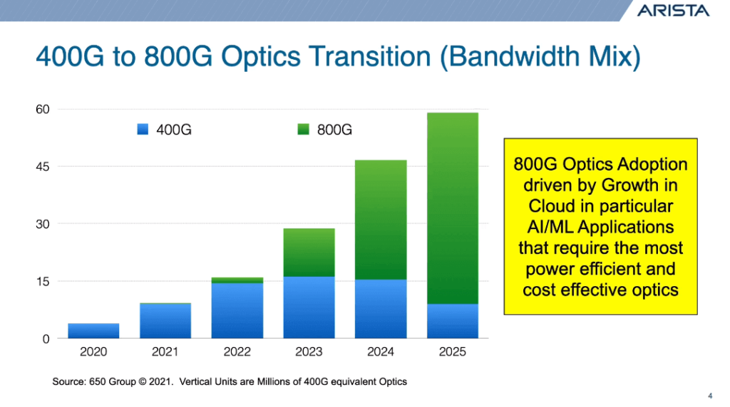
Why Choose 800G Optics?
1. Cost Reduction: 800G optics can save costs at the optical and system level, such as reducing the use of optical fiber, lowering the number of optical modules, and improving the integration and reliability of the system. In addition, 800G optical devices can also utilize the existing 100G and 400G technology and equipment to reduce the cost of R&D and production.
2. Reduced power consumption: 800G optical devices can achieve energy savings at the optical and system level, such as using more efficient modulation formats, optimizing circuit design, and reducing power density. According to a study, the power consumption of 800G optical modules is about 30% lower than that of 400G optical modules.
3. Higher density: 800G optics can increase the transmission density of the network to meet the high demand for bandwidth in scenarios such as data centers and cloud computing. For example, 800G optical modules can realize a transmission rate of 800Gbps per wavelength, which is equivalent to eight 100Gbps or two 400Gbps. This can improve the utilization rate of switch chips and keep up with the switch chip roadmap.
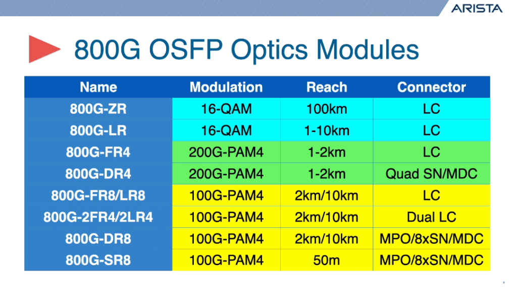
800G OSFP Optical Transceiver Modules
800G Breakout Applications
1. 800G breakout technology enables efficient combinations of multiple use cases, supports aggregation and shuffle, and improves fault tolerance and flexibility of the network while increasing the number of ports and bandwidth of the switch.
2. 800G to Dual 400G-DR4/FR4/LR4/ER4 breakout technology enables interconnection between two 400G optical modules, covering different transmission distances and scenarios and reducing cost and complexity by utilizing dual LC, dual Mini-LC or dual MPO, which are common fiber connectors.
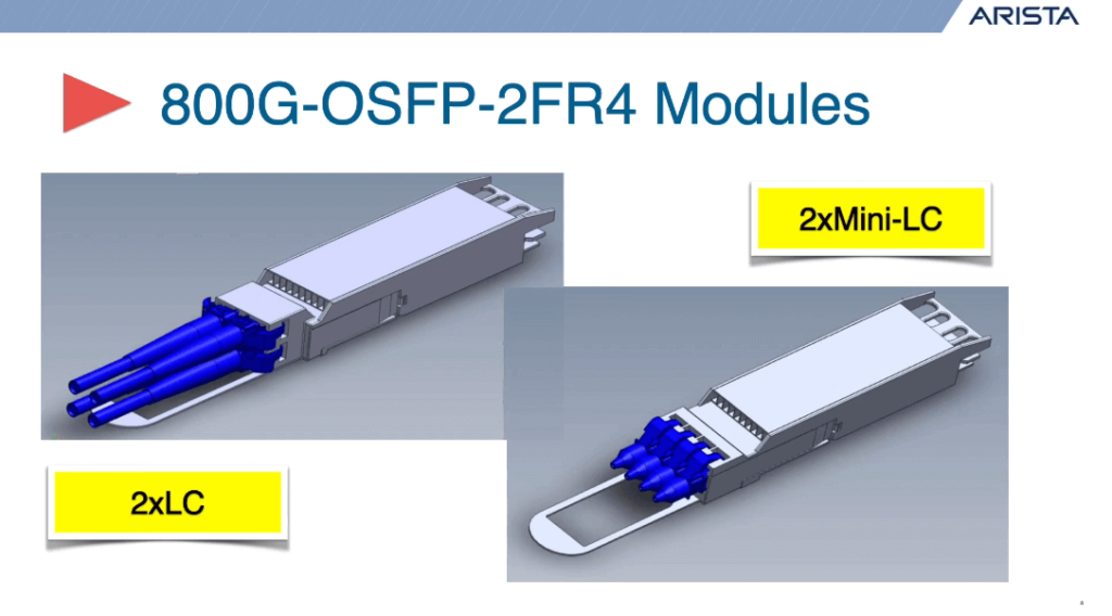
3. 800G DR8 breakout technology can break down an 800G optical module into octal 100G DR optical modules, using octal SN/MDC, a new type of ultra-compact connector, to achieve high-density fiber optic cabling to meet the high traffic demand of data centers.
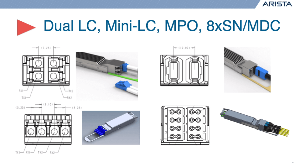
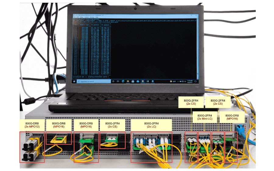
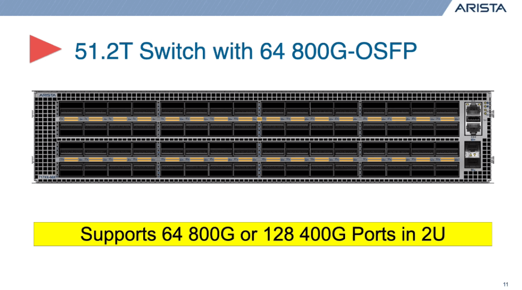
200G Lambda Optics
200G Lambda is an emerging optical transmission technology that can achieve a data rate of 200Gbps per wavelength on a single fiber, which has the following advantages over the traditional multi-wavelength 100G technology:
1. Lower Power Consumption per Bit: 200G Lambda technology saves 20% to 30% of power consumption because it requires only one laser and one optical receiver, as opposed to four lasers and four optical receivers for multi-wavelength 100G technology. In addition, 200G Lambda technology reduces power consumption by reducing circuit complexity and signal processing overhead.
2. Reduced Cost Per Bit: 200G Lambda technology can reduce the cost per bit by 50% because it reduces the number and cost of lasers and fiber terminations, as well as the number and cost of optical modules and fiber links. Also, 200G Lambda technology can utilize existing 100G technology and equipment, reducing the cost of R&D and production.
3. The best choice for 200G SerDes in the future: SerDes are circuits that convert serial data to parallel data, or parallel data to serial data, and perform high-speed data communication between the switch chip and the optical module. 200G Lambda technology requires only one 200G SerDes channel for 200Gbps data transmission, while the multi-wavelength 100G technology requires four 100G SerDes channels to realize the same data transmission.
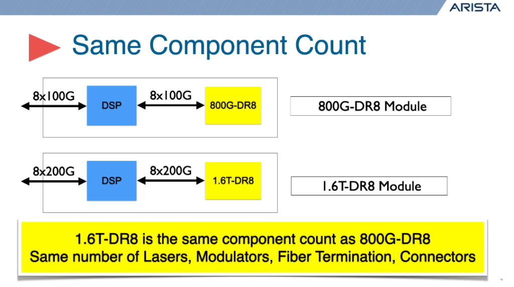
Current Status of 200G Lambda
1. Technical feasibility has been established for a variety of optical technologies such as EML and SiPh.
2. Need to finalize new FEC and optical specifications for 200G Lambda specification.
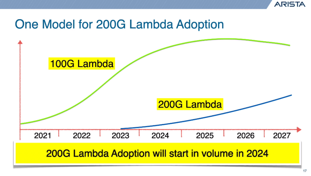
Need for multi-vendor 200G Lambda specification to allow continued implementation of 200G Lambda gearboxes. 200G Lambda adoption will start in volume in 2024.
1.6T Pluggable Optical Transceiver Module
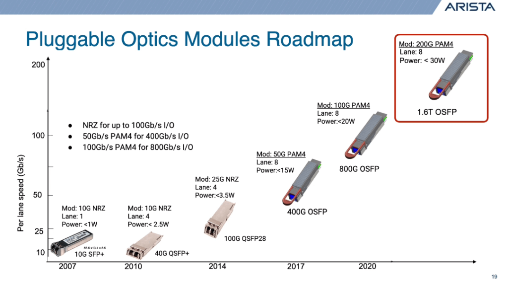
Pluggable Optical Module Technology Roadmap
The 1.6T-OSFP (8x200G channels) is a high-speed optical module that provides eight 200G channels of optical signals on a single OSFP interface to achieve a total bandwidth of 1.6Tb/s. The module is designed to be used in a wide range of applications, such as in the field of optical fiber optics. This optical module utilizes PAM4 modulation technology, which uses 50G of electrical signals per channel to drive 100G of optical signals. To ensure electrical performance at 200G/channel, the OSFP MSA 200G Working Group fine-tuned the dimensions and electrical specifications of the OSFP interface in October 2020, making the 1.6T-OSFP optical module fully compatible with the 800G OSFP optical module. This compatibility provides more flexibility and scalability for data center networks. In connection with 200G SerDes switch chips, 1.6T OSFP optical modules can be directly connected to switch chips using 200G SerDes technology without the need for additional converters or adapters. This reduces network cost and power consumption and improves network efficiency. It is expected that 200G SerDes switch chips will become the mainstream choice for data center networks by 2025.
OSFP
Octal Small Form Factor Pluggable, XD=Extra Dense
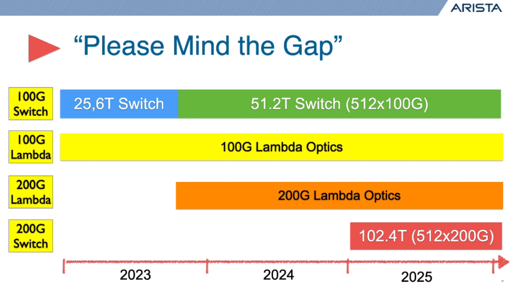
As the demand for high-speed data transmission in data center networks continues to grow, there has been a strong interest in 1.6T optical modules. Combined with a 51.2T switch chip, the 1.6T optical module can achieve 51.2T switch density in a 1U line card or fixed chassis, dramatically reducing system-level costs. This switch chip utilizes 100G SerDes technology, which means that each channel can carry 100Gbps of data. This SerDes technology has become a mainstream choice in the market and more switch chips are expected to utilize 100G SerDes technology between 2023 and 2027.
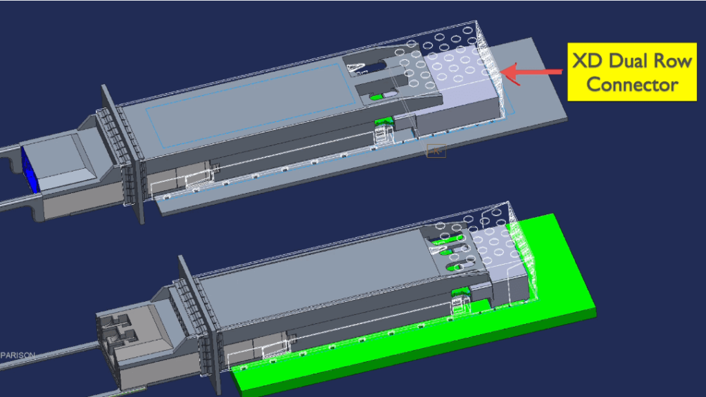
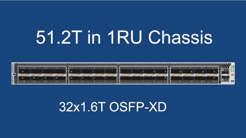
OSFP-XD (Ultra High Density) is a new type of optical module with the following features:
1. It supports 16 electrical channels, each of which can reach 100G or 200G, resulting in a total data rate of 1.6T or 3.2T.
2. It has efficient power management, requiring only 33W of power to support a variety of optical solutions, including single-mode fiber, multi-mode fiber, and active fiber optic cable.
3. It features a high-density package design with the same form factor as the OSFP (eight-channel small form-factor pluggable) but with higher-density connectors and cable assemblies. This makes it compatible with stacked 800G-OSFPs, greatly simplifying market acceptance and deployment.
4. It has flexible compatibility in that it can coexist with stacked OSFP (two-channel small form-factor pluggable) on a single motherboard, providing more configuration options and expansion capabilities.
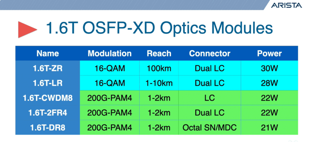
The Differences of 1.6T OSFP Optical Module
Advantages of QSFP-XD
1. It is the densest pluggable optical solution on the market today, and it supports 16 electrical channels, each of which can reach 100G or 200G, resulting in a total data rate of 1.6T or 3.2T. It has the same form factor as the OSFP ( Octal Small Form Factor Pluggable) but utilizes a higher-density connector and cable assembly. This makes it compatible with stacked 800G OSFP, greatly simplifying market acceptance and deployment. It meets future chip density growth requirements and improves system throughput and efficiency.
2. It supports a full range of optical technologies, including 100G Lamdba, 200G Lambda, and Coherent, which can be adapted to different transmission distances and scenarios. It can support transmission distances of up to 2 kilometers at a temperature range of 0-70°C with a low power consumption of less than 23W. It enables high-speed, efficient, and highly reliable data transmission to meet the needs of data centers, cloud computing, artificial intelligence, and other fields.
3. It retains all the benefits of a pluggable optical module, including configurability, serviceability, technical flexibility, and more. It also retains the well-known supply chain business model, allowing customers to choose the most appropriate products and services from multiple vendors.
How to Reduce Power Consumption Per Bit

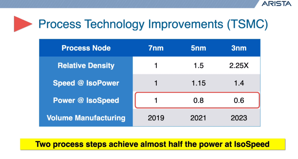
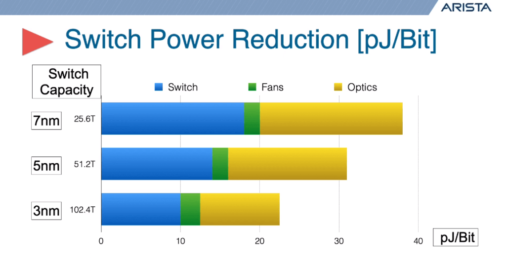
Process Technology Improvement (TSMC)
The 3NM process achieves almost half the power reduction at IsoSpeed compared to the 7NM process.
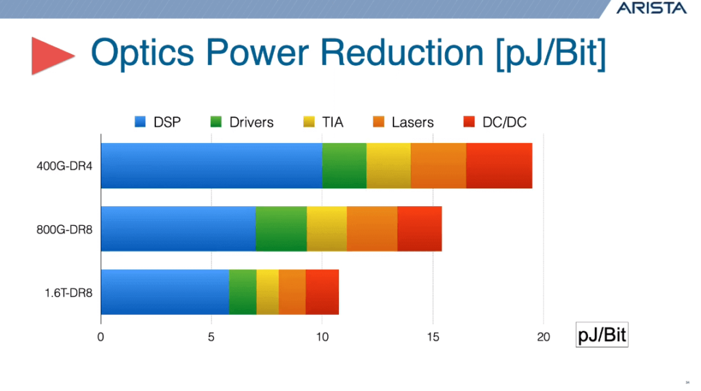
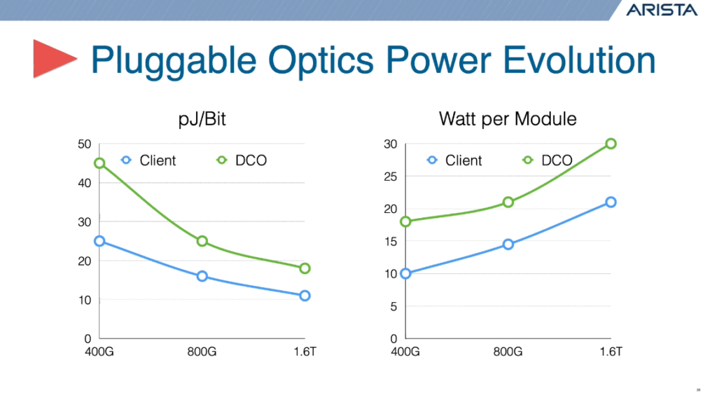
Pluggable optics power evolution
Though the power consumption of individual modules is rising from 400G-1.6T, the average power consumption per bit is decreasing significantly.
Ways to Further Reduce Power Consumption
1. Utilize 3nm and 2nm DSP technologies: These advanced digital logic technologies can dramatically reduce the size and resistance of transistors, thereby reducing the switching losses and static power consumption of the circuit.
2. Designing low-power SerDes interfaces: SerDes are interfaces that convert serial data into parallel data and are commonly used for high-speed communications. We can reduce the power consumption of SerDes by optimizing coding, modulation, and filtering while ensuring signal integrity and reliability.
3. Uses low-power optical modulators: Optical modulators are devices that use photonics to control optical signals and are commonly used in fiber optic communications. We can reduce the drive voltage and insertion loss of optical modulators by improving the optical waveguide, electrodes, and materials to reduce power consumption.
There is still much room for innovation in the future, including the realization of single-wavelength 200G transmission, the development of lasers with better performance, and the reduction of losses in the coupling and modulation process. The goal for the next five years is to reduce energy consumption to 5 to 6 pJ per bit, which will require the use of digital signal processors on 2nm processes, improving the efficiency of lasers and modulators, and reducing coupling losses between the laser and the waveguide.
All optics benefit from reduced power consumption. Improvements in optical power are largely independent of form factor.
Pluggable optical modules provide a smooth upgrade path to existing high-volume platforms, allowing advances in low-power optics to reach the market quickly and in high volumes.
Power Consumption Summary
1. Power consumption per bit for switches is decreasing significantly, roughly a factor of 2X for every two process generations.
2. Power consumption per bit for optical modules is also decreasing significantly, roughly a factor of 2X for every two process generations.
3. Power per optical module is increasing, with capacity growing from 400G->800G->1.6T.
4. Power targets for 1.6T modules: 20-25W for client optics, 25-30W for DCI optics.
5. Robust thermal form factor required for 20-30W: OSFP provides appropriate packaging.
6. Further power reduction needed: 3/2nm DSPs, lower power Serdes, and modulators.
Analysis of CPO and Pluggable
CPO (co-packaged optics) is a technology that tightly integrates an optical transceiver or optical engine with a switching chip, which can increase the speed and density of data transmission and reduce power consumption and latency. Currently, CPO technology has demonstrated some results in the labs of companies such as Facebook and Microsoft and is also supported and promoted by industry organizations such as OIF (Optical Interconnect Forum). However, CPO still faces a considerable number of challenges, such as how to increase the power and efficiency of lasers, how to reduce fiber and connector losses and failures, how to ensure the manufacturability, repairability, and maintainability of CPO modules, as well as how to control the cost and power consumption, and so on.
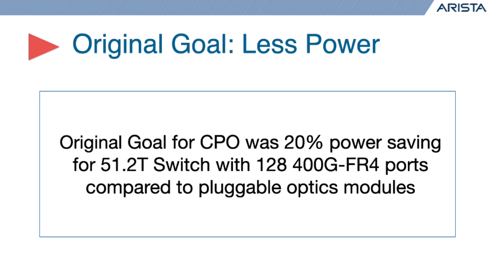
VSR Replaces XSR SERDES. Chip vendors have added a low-power VSR SERDES mode to their switch chips, enabling the 51.2T switch chip to realize 180W of wall-plug energy savings compared to LR SERDES.
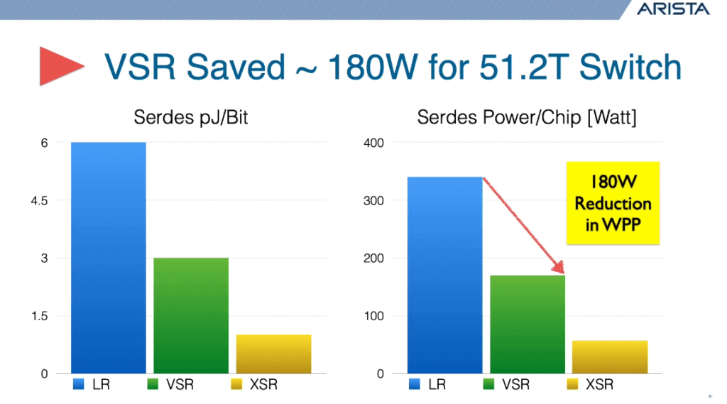
VSR saved about 180W for the 51.2T switch
VSR levels the playing field. While the 180W power savings are good news, the same low-power VSR SERDES interface can be used with pluggable optical modules.
The result: CPOs and pluggable optics modules have the same electrical link power.

CPO + ELS Increases Power. The CPO’s External Light Source (ELS) introduces additional optical coupling losses, which increase the laser power compared to conventional pluggable optical modules, making the CPO+ELS higher power than pluggable optical modules.
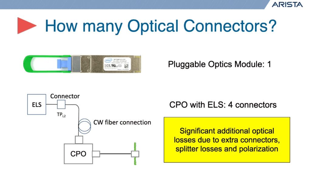
Pluggable modules have one optical connector and CPO modules have four optical connectors, which results in significant additional optical loss due to additional connector splitter loss and polarization.
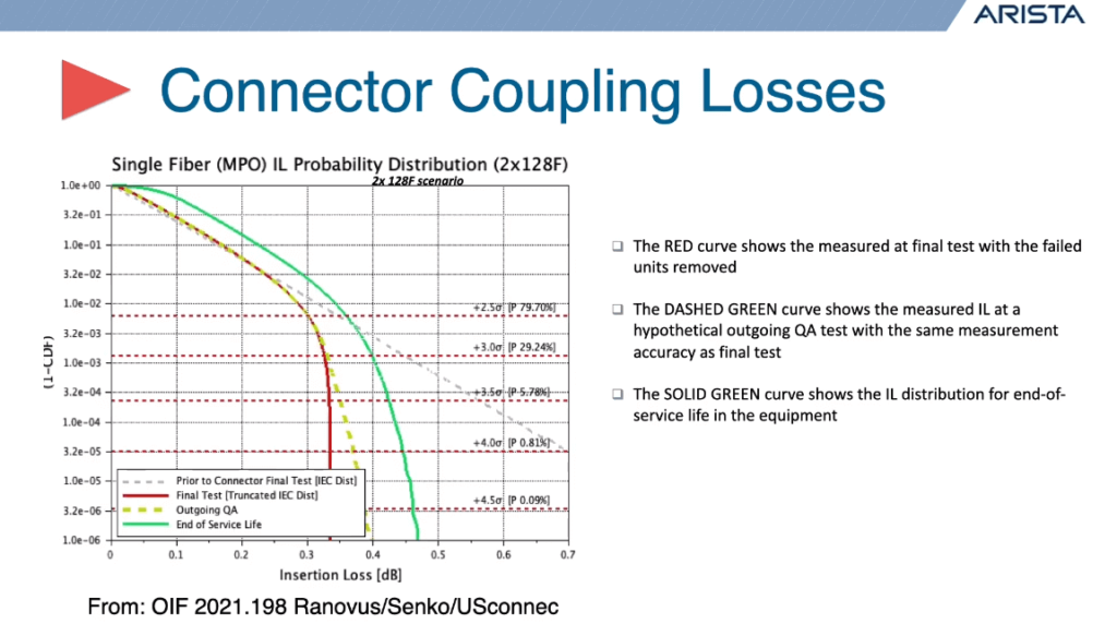
Coupling Losses vs. Pluggable
1. Additional Connector Losses: 1.2-1.6 dB
Most likely need expanded beam connectors for ELS.
2. Splitter and Polarization Losses: 0.6-1.2 dB
Very hard to minimize these for a large number of fibers.
6. Total Additional Coupling Losses: 1.8-3 dB
Increases laser power by 50% to 100%.
Further Power Reduction Needed
1. Direct Drive Reduces Power by Eliminating DSP
Challenging to make this a multi-vendor standard.
2. Very Hard to Reduce Laser Power with ELS
Additional coupling losses increase laser power.
3. Alternative Modulation Technologies
Silicon Photonics Modulators have high insertion loss.

CPO Summary
1. CPO is not required for 51.2T or 102.4T Switches
The problem has been solved with Pluggable Optics.
2. 800G and 1600G Pluggable Optics have no risk
No design, serviceability, or manufacturability issues.
3. Today’s CPO are not saving Power over Pluggable
Most promising future direction for CPO is direct-drive.
Related Products:
-
 QSFP28-100G-IR4 100G QSFP28 IR4 1310nm (CWDM4) 2km LC SMF DDM Transceiver Module
$110.00
-
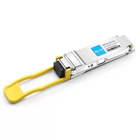 QSFP28-100G-DR1 100G QSFP28 Single Lambda DR 1310nm 500m LC SMF with FEC DDM Optical Transceiver
$180.00
-
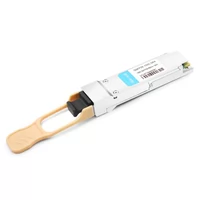 QSFP28-100G-SR4 100G QSFP28 SR4 850nm 100m MTP/MPO MMF DDM Transceiver Module
$40.00
-
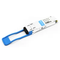 QSFP28-100G-LR4 100G QSFP28 LR4 1310nm (LAN WDM) 10km LC SMF DDM Transceiver Module
$285.00
-
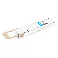 OSFP-400G-SR4-FLT 400G OSFP SR4 Flat Top PAM4 850nm 30m on OM3/50m on OM4 MTP/MPO-12 Multimode FEC Optical Transceiver Module
$650.00
-
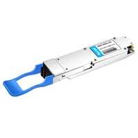 OSFP-400G-LR4 400G LR4 OSFP PAM4 CWDM4 LC 10km SMF Optical Transceiver Module
$1199.00
-
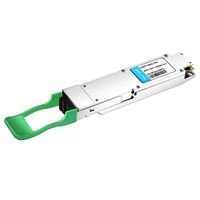 OSFP-400G-FR4 400G FR4 OSFP PAM4 CWDM4 2km LC SMF FEC Optical Transceiver Module
$900.00
-
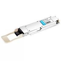 OSFP-400G-SR8 400G SR8 OSFP PAM4 850nm MTP/MPO-16 100m OM3 MMF FEC Optical Transceiver Module
$480.00
-
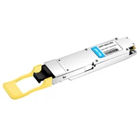 OSFP-800G-DR8 OSFP 8x100G DR PAM4 1310nm MPO-16 500m SMF DDM Optical Transceiver Module
$1100.00
-
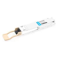 OSFP-800G-SR8 OSFP 8x100G SR8 PAM4 850nm MTP/MPO-16 100m OM4 MMF FEC Optical Transceiver Module
$750.00
-
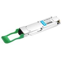 OSFP-800G-2FR4 OSFP 2x400G FR4 PAM4 CWDM4 2km DOM Dual CS SMF Optical Transceiver Module
$3500.00
-
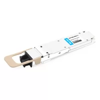 OSFP-800G-SR8D-FLT OSFP 8x100G SR8 Flat Top PAM4 850nm 100m DOM Dual MPO-12 MMF Optical Transceiver Module
$850.00
-
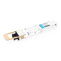 NVIDIA MMA4Z00-NS Compatible 800Gb/s Twin-port OSFP 2x400G SR8 PAM4 850nm 100m DOM Dual MPO-12 MMF Optical Transceiver Module
$750.00
-
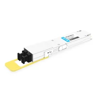 NVIDIA MMS4X00-NM-FLT Compatible 800G Twin-port OSFP 2x400G Flat Top PAM4 1310nm 500m DOM Dual MTP/MPO-12 SMF Optical Transceiver Module
$1200.00
-
 NVIDIA MMA4Z00-NS-FLT Compatible 800Gb/s Twin-port OSFP 2x400G SR8 PAM4 850nm 100m DOM Dual MPO-12 MMF Optical Transceiver Module
$850.00
-
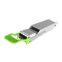 OSFP-XD-1.6T-4FR2 1.6T OSFP-XD 4xFR2 PAM4 1291/1311nm 2km SN SMF Optical Transceiver Module
$17000.00
-
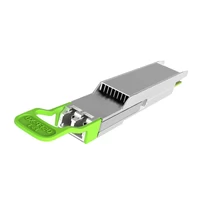 OSFP-XD-1.6T-2FR4 1.6T OSFP-XD 2xFR4 PAM4 2x CWDM4 TBD Dual Duplex LC SMF Optical Transceiver Module
$22400.00
-
 OSFP-XD-1.6T-DR8 1.6T OSFP-XD DR8 PAM4 1311nm 2km MPO-16 SMF Optical Transceiver Module
$12600.00
