HBM, short for High Bandwidth Memory, is a high-performance 3D-stacked DRAM technology primarily used to meet the high demands for memory bandwidth and capacity of high-performance computing and graphics processing units (GPUs). The HBM technology was co-developed by AMD and Hynix and was first announced in 2013.
As computational demands continue to grow, traditional memory technologies have struggled to meet the increasing needs for memory bandwidth and capacity required by high-performance computing (HPC) and GPUs. Against this backdrop, High Bandwidth Memory (HBM) technology emerged as an innovative solution to address these challenges.
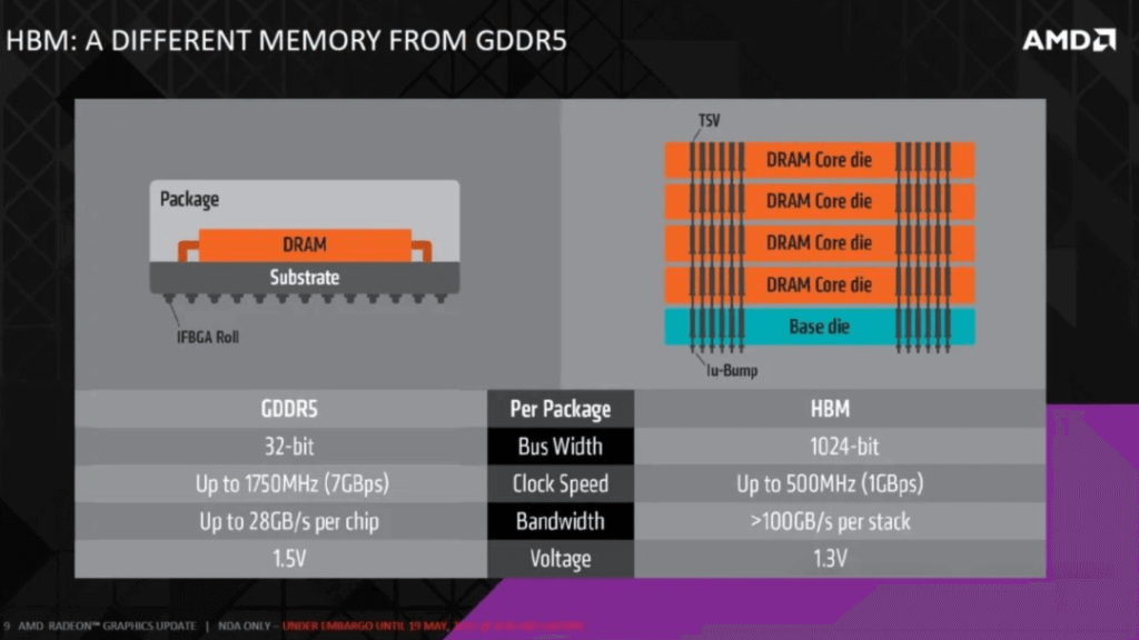
HBM is a 3D-stacked DRAM technology that vertically interconnects multiple DRAM chips stacked together using high-density Through-Silicon Vias (TSVs) and microbump technologies. This design significantly enhances memory bandwidth and capacity while reducing the physical size of the memory modules. Compared to traditional GDDR5 memory, HBM typically has lower power consumption due to its compact design and efficient data transfer.
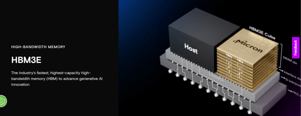
Currently, HBM products have been developed in the order of HBM (first generation), HBM2 (second generation), HBM2E (third generation), HBM3 (fourth generation), and HBM3E (fifth generation), with the latest HBM3E being an extended version of HBM3. GPUs now commonly feature 2/4/6/8 stacks of HBM, with up to 12 layers stacked in three dimensions.
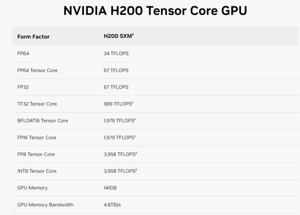
On February 26, Micron Technology officially announced the mass production of HBM3E high-bandwidth memory. Its 24GB 8H HBM3E product will be supplied to NVIDIA and applied to NVIDIA’s H200 Tensor Core GPU. Micron’s HBM3E currently has a 24GB capacity, with a pin speed exceeding 9.2Gb/s, providing over 1.2TB/s of memory bandwidth, offering lightning-fast data access speeds for AI accelerators, supercomputers, and data centers.
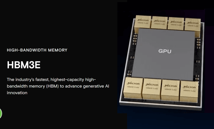
Currently, mainstream AI training chips all utilize HBM, with one GPU paired with multiple HBMs. Taking NVIDIA’s newly released H200 as an example, this GPU is equipped with six Micron HBM3E 24GB high-speed memory modules. Logically, the H200’s memory capacity should be 246=144GB, and the memory bandwidth should be 1.26=7.2TB/s. However, the specifications released on NVIDIA’s official website show only 141GB of memory, not an integer, and the memory bandwidth is only 4.8TB/s. This is due to mass production reasons, where NVIDIA reserves a small portion as redundancy to improve the yield rate.
HBM is continuously evolving, with the direction of iteration aimed at increasing capacity and bandwidth. Currently, the highest number of layers is 12. SK Hynix launched the world’s first HBM in 2014, followed by HBM2 in 2018, and has been releasing a new generation of HBM every two years since then. The latest mass-produced version is HBM3e, and the original manufacturer is accelerating research and development, with HBM4 possibly adopting a 16-layer stack. In terms of I/O count (bus width), HBM1 to HBM3e all maintain 1024 bits, while the data transfer rate has increased from 1Gb/s for HBM1 to 9.2Gb/s for HBM3e, ultimately achieving a bandwidth increase from 128GB/s for HBM1 to 1.2TB/s for HBM3e. The standards for HBM4 are currently undetermined, but it is generally expected that HBM4 will have a maximum of 16 layers stacked and a 2048-bit bus width.
The HBM market is mainly dominated by three major storage giants:
SK Hynix: As one of the main developers of HBM technology, SK Hynix holds a leading position in the HBM field. The company not only participated in the early development of HBM but also continues to drive the iteration of the technology, such as HBM2, HBM2E, and HBM3. SK Hynix’s innovation and mass production capabilities in HBM technology have made it the main supplier of HBM for NVIDIA’s AI chips, with the highest market share.

Samsung Electronics: Samsung Electronics is one of the world’s leading semiconductor companies and also has strong R&D and production capabilities in HBM technology. Samsung Electronics has invested heavily in the development of HBM and actively expanded its production capacity to meet market demand. Samsung’s progress in HBM technology, including the development of higher-density and larger-capacity products, has played a key role in enhancing its competitiveness in high-performance computing and AI. Samsung focuses on fulfilling orders from other cloud service providers, and under increased customer orders, it is expected that the market share gap between Samsung and SK Hynix in HBM3 will significantly narrow, with an estimated equal market share for both companies in 2023-2024, collectively holding about 95% of the HBM market share.
Micron Technology: Micron has a relatively low market share in the HBM market due to misjudgments in technology direction and is in the process of catching up. Although Micron entered the HBM market later than SK Hynix and Samsung Electronics, it started directly with HBM3E and quickly enhanced its technological strength, posing a challenge to the existing market structure. NVIDIA’s use of Micron in the H200 is a significant recognition of its capabilities.
Related Products:
-
 OSFP-800G-FR4 800G OSFP FR4 (200G per line) PAM4 CWDM Duplex LC 2km SMF Optical Transceiver Module
$3500.00
OSFP-800G-FR4 800G OSFP FR4 (200G per line) PAM4 CWDM Duplex LC 2km SMF Optical Transceiver Module
$3500.00
-
OSFP-800G-2FR2L 800G OSFP 2FR2 (200G per line) PAM4 1291/1311nm 2km DOM Duplex LC SMF Optical Transceiver Module
$3000.00
-
OSFP-800G-2FR2 800G OSFP 2FR2 (200G per line) PAM4 1291/1311nm 2km DOM Dual CS SMF Optical Transceiver Module
$3000.00
-
OSFP-800G-DR4 800G OSFP DR4 (200G per line) PAM4 1311nm MPO-12 500m SMF DDM Optical Transceiver Module
$3000.00
-
NVIDIA MMS4X00-NM-FLT Compatible 800G Twin-port OSFP 2x400G Flat Top PAM4 1310nm 500m DOM Dual MTP/MPO-12 SMF Optical Transceiver Module
$1199.00
-
NVIDIA MMA4Z00-NS-FLT Compatible 800Gb/s Twin-port OSFP 2x400G SR8 PAM4 850nm 100m DOM Dual MPO-12 MMF Optical Transceiver Module
$650.00
-
NVIDIA MMS4X00-NM Compatible 800Gb/s Twin-port OSFP 2x400G PAM4 1310nm 500m DOM Dual MTP/MPO-12 SMF Optical Transceiver Module
$900.00
-
NVIDIA MMA4Z00-NS Compatible 800Gb/s Twin-port OSFP 2x400G SR8 PAM4 850nm 100m DOM Dual MPO-12 MMF Optical Transceiver Module
$650.00
-
NVIDIA MMS1Z00-NS400 Compatible 400G NDR QSFP112 DR4 PAM4 1310nm 500m MPO-12 with FEC Optical Transceiver Module
$700.00
-
NVIDIA MMS4X00-NS400 Compatible 400G OSFP DR4 Flat Top PAM4 1310nm MTP/MPO-12 500m SMF FEC Optical Transceiver Module
$700.00
-
NVIDIA MMA1Z00-NS400 Compatible 400G QSFP112 VR4 PAM4 850nm 50m MTP/MPO-12 OM4 FEC Optical Transceiver Module
$550.00
-
NVIDIA MMA4Z00-NS400 Compatible 400G OSFP SR4 Flat Top PAM4 850nm 30m on OM3/50m on OM4 MTP/MPO-12 Multimode FEC Optical Transceiver Module
$550.00
-
NVIDIA MMS4X50-NM Compatible OSFP 2x400G FR4 PAM4 1310nm 2km DOM Dual Duplex LC SMF Optical Transceiver Module
$1200.00
-
OSFP-XD-1.6T-4FR2 1.6T OSFP-XD 4xFR2 PAM4 1291/1311nm 2km SN SMF Optical Transceiver Module
$15000.00
-
OSFP-XD-1.6T-2FR4 1.6T OSFP-XD 2xFR4 PAM4 2x CWDM4 2km Dual Duplex LC SMF Optical Transceiver Module
$20000.00
-
OSFP-XD-1.6T-DR8 1.6T OSFP-XD DR8 PAM4 1311nm 2km MPO-16 SMF Optical Transceiver Module
$12000.00