As chip manufacturing processes continue to shrink, the impact of interconnects on chip performance becomes increasingly significant. Interconnects act as the internal “streets” and “highways” within microelectronic devices, connecting components like transistors, resistors, and capacitors. As chips get smaller, interconnects must become finer, but this reduction in spacing can lead to parasitic effects affecting circuit performance. Common interconnect materials, such as aluminum, copper, and carbon nanotubes, face physical limitations. However, silicon photonics offers a solution.
Silicon photonics leverages silicon as an optical medium, using laser beams instead of electronic semiconductor signals for data transmission. It’s a next-generation technology based on silicon and silicon-on-insulator (SOI) substrates, integrated using existing CMOS processes. The key advantage lies in its high transmission rates, enabling data transfer between processor cores at speeds up to 100 times faster than traditional electronic interconnects. Additionally, silicon photonics achieves excellent power efficiency, making it a promising semiconductor technology.
Historically, silicon photonics developed on SOI wafers, but their high cost and limitations for various photonic functions prompted the exploration of alternative materials. Researchers have now developed new materials like LNO films, InP, BTO, polymers, and plasma materials to achieve even higher performance. Silicon photonics holds great promise for addressing interconnect challenges and advancing semiconductor technology.
Silicon photonics, the study and application of photonic systems using silicon as an optical medium, has become a mainstream technology driven by advances in optical communications. Despite the initial intuition that electronic fabrication processes couldn’t directly integrate photonics, recent developments have defied this notion. Let’s explore why we’re fortunate that these capabilities can now be leveraged for photonics.
In reality, direct reuse isn’t straightforward. Attempts to integrate photonics functionality into existing CMOS or bipolar silicon wafers without process modifications resulted in underperforming devices. Electronic processes are tailored for manufacturing electronic products, making them ill-suited for competitive photonics products. Even if feasible, the economic viability is questionable. Silicon photonics chips require relatively primitive processing capabilities (around 90 nanometers), compared to advanced microelectronics (such as 16 nanometers). Attempting to build photonics using cutting-edge microelectronic tools would be both impractical and economically unproven. There’s no reason to expect that integrated processes designed for electronic circuits would seamlessly align with components manipulating light.
Over the past decade, silicon has proven to be an excellent material not only for electronic devices but also for photonics components. Even more astonishingly, the silicon photonics community has developed processes that allow reusing CMOS manufacturing infrastructure to construct complex photonic circuits. While the complete integrated process for transistor manufacturing isn’t directly reused, modular steps can be rearranged and repurposed for silicon photonics. Several organizations have demonstrated the feasibility of this approach. They leverage materials and techniques developed over the past 50 years in silicon microelectronics to build photonic devices and circuits. What’s remarkable is that many efforts don’t merely use similar equipment in separate facilities; they employ the same tools and facilities used to build conventional CMOS transistors. However, working within these facilities comes with significant constraints: unverified materials incompatible with CMOS processes are prohibited, and circuit designs must avoid damaging or contaminating the tools. In more advanced CMOS-compatible manufacturing facilities, mask sets and process development costs can be prohibitively high, especially for cutting-edge processes.
Despite these challenges, the massive investments in constructing modern CMOS factories can now directly benefit silicon photonics. This opens up an immediately available, commercially viable path for large-scale production. By sharing mature semiconductor industry infrastructure, silicon photonics is gradually becoming the critical bridge connecting future high-speed data communication, computing, and sensing applications.
The Evolution of Silicon Photonics
Silicon photonics is a technology that leverages silicon as an optical medium to create photonic systems. Its history dates back to the late 1980s and early 1990s, with several stops and starts along the way. However, it has now emerged as a prominent field with significant potential.
In traditional communication systems, different materials are used for various components. These chips often contain a mix of materials, such as RF CMOS or bipolar processes for broadband electronic devices (e.g., serializers and deserializers), highly scaled CMOS or FPGAs for digital parts (e.g., control circuits), glass-based diffused waveguides for passive elements, lithium niobate (LiNbO₃) for modulators, indium phosphide (InP) for lasers, germanium (Ge) for photodetectors, and MEMS-based switches. Each material system is chosen to optimize performance for a specific device type.
However, the specialized manufacturing processes for each component lead to low yields and high costs. Photonics devices are often produced in low quantities using dedicated fabrication equipment, making them expensive compared to large-scale electronic production. While discrete photonics components can be interfaced using standard optical fibers and connectors, the cost and yield losses primarily stem from photonics packaging processes. These processes require precise alignment (often involving 5-axis or 6-axis alignment) at sub-micrometer levels and sometimes hermetic sealing or even gold plating.
The immense potential of silicon photonics lies in integrating multiple functionalities into a single package. By using the same manufacturing facilities as advanced microelectronics, it becomes possible to create hybrid chips or chip stacks where both optical and electronic components coexist. This fundamental integration significantly reduces the cost of transmitting data via optical fibers. Moreover, it opens up opportunities for novel applications, allowing the construction of complex systems at a reasonable cost.
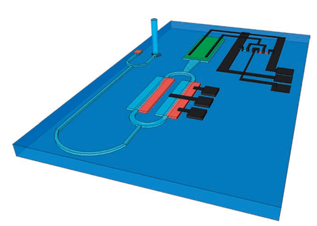
Light is coupled into the photonic circuit through on-chip lasers or vertical optical fibers, which then modulate the light. The modulated light is converted by photodetectors and inverted using CMOS complementary circuits. Silicon photonic electronic circuits now support systems composed of hundreds or thousands of such components.
Applications
Complex silicon photonic systems are finding numerous applications, with data communication being the most common. This includes high-bandwidth digital communication for short-distance applications, sophisticated modulation schemes for long-distance applications, and coherent communication. Beyond data communication, both industry and academia are exploring a wide range of new applications for this technology. These applications include nano optomechanics and condensed matter physics, biosensing, nonlinear optics, laser radar systems, optical gyroscopes, RF-integrated optoelectronics, integrated radio transceivers, coherent communication, novel light sources, laser noise reduction, gas sensors, extremely long-wavelength integrated photonics, high-speed and microwave signal processing, among others. Particularly promising areas include biosensing, imaging, laser radar, inertial sensing, hybrid photonic-RF integrated circuits (RFICs), and signal processing.
Data Communication
Among various categories of photonic devices, silicon photonic components compete favorably with their counterparts. One of the most transformative efforts in the field of optical communication is the creation of integrated platforms that integrate modulators, detectors, waveguides, and other components on the same chip, allowing them to communicate with each other. In some cases, transistors are also included in these platforms, enabling amplification, serialization, and feedback to be integrated on the same chip. Due to the cost of developing such processes, this endeavor primarily targets point-to-point data communication applications. Additionally, due to the cost of developing transistor manufacturing processes, the emerging consensus in this field is that, from a performance and cost perspective, it is most meaningful to integrate electronic devices using bonding techniques at the wafer or chip level in the foreseeable future.
The ability to create chips that can perform computation using electronic devices and carry out optical communication holds significant value. Most early applications of silicon photonics have been in digital data communication. This is driven by the fundamental physical differences between electrons (fermions) and photons (bosons). Electrons are well-suited for computation because two of them cannot simultaneously occupy the same location. This strong mutual interaction between electrons allows for the construction of large-scale nonlinear switching devices—transistors.
Photons exhibit different properties: many photons can coexist in the same location simultaneously, and under very special conditions, they do not interfere with each other. This is why it is possible to transmit trillions of bits of data per second through a single optical fiber: it is not achieved by creating a single trillion-bit bandwidth data stream.
In many regions around the world, fiber-to-the-home (FTTH) is the dominant access paradigm, although in the United States, it has not yet been proven correct due to competition with DSL and other technologies. As the demand for bandwidth continues to grow, the need for more efficient data transmission through optical fibers is steadily increasing. A widespread trend in the data communication market is that as distances shorten, the price per unit decreases sharply while the quantity increases. It is no surprise that commercial efforts in silicon photonics have focused extensively on high-capacity, short-distance applications, targeting data centers and high-performance computing. Future applications will include board-to-board and USB-scale short-distance connections, and eventually, perhaps even core-to-core communication within CPUs, although the latter remains speculative for on-chip core-to-core applications. Although silicon photonics has not yet reached the scale of the CMOS industry, it has already become an important field.
Waveguides and Passive Components
In silicon-compatible systems, various geometries of waveguides have been developed. Nearly all transparent materials with refractive indices higher than glass can be deposited onto silicon dioxide substrates to form waveguides. However, to achieve compatibility with CMOS processes, the industry has converged on several geometric shapes. The most common is the high-consistency waveguide made from the active device layer of silicon-on-insulator (SOI) wafers. This type of waveguide can be fully etched down to the bottom oxide layer or partially etched (using timed processes) .
Reducing the losses in these submicron waveguides to acceptable levels has required years of effort. The strong interaction between the optical field and sidewalls leads to significant losses due to surface roughness. Propagation losses can be minimized by optimizing the process to smooth the sidewalls or adjusting the waveguide geometry to reduce the sidewall modal field strength. Other critical passive components, such as grating couplers, distributed Bragg gratings, waveguide crossings, and arrayed waveguide gratings (AWGs), have also demonstrated very low losses in each case. Recently, CMOS-compatible waveguides formed in the back-end-of-line process using silicon nitride have emerged. These waveguides exhibit very low losses (< 0.1 dB/m), but their compatibility with front-end active devices remains an open question due to the high-temperature growth required. Notably, significant progress has been made in low-loss silicon waveguides. However, manufacturing compatible high-speed modulators and detectors on these platforms presents considerable challenges, making large-scale integration less optimistic. One of the challenges faced by silicon photonics technology is the optical coupling between chips and optical fibers, which requires cost-effective packaging methods.
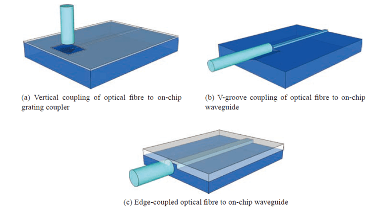
This is typically achieved using edge couplers or grating couplers, as shown in the Figure. Both methods have been proven to have losses below 1 dB per interface. Handling polarization is also a challenge because silicon photonic waveguides inherently exhibit strong birefringence, meaning that the propagation constants for two different polarizations of light in the waveguide are different. A common practice is to construct circuits using a single polarization and replicate these circuits when both polarizations are needed. This approach, known as polarization diversity, leverages the advantages of polarization-splitting grating couplers, polarization splitters, polarization rotators, or other related components. Other methods have explored the use of rectangular waveguides to mitigate birefringence, but these approaches impose significant design constraints.
Modulator
Achieving modulation in silicon is typically done through the plasma dispersion effect, where changes in the free carrier density cause refractive index variations and modulate light. Several different mechanisms to manipulate free carrier density have been implemented in single-chip devices. Among these, carrier-depletion-mode devices based on reverse-biased PN junctions are widely used for high-speed operation.
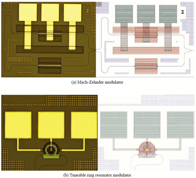
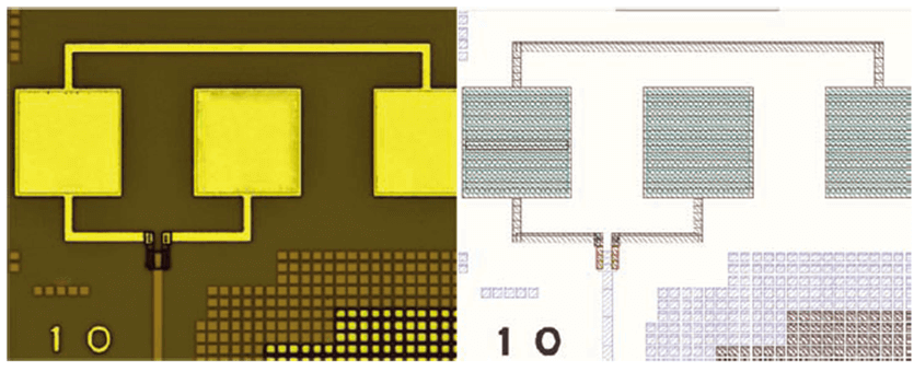
Since Intel’s team first demonstrated GHz silicon modulators, the performance metrics of modulators have significantly improved. The Mach-Zehnder interferometer (MZI) structure is commonly used for amplitude modulation. The figure below shows an example of an MZI modulator.
Resonant structures can be used to significantly reduce device size and further lower power consumption, although this significantly narrows the operating wavelength window and increases thermal sensitivity. High-speed ring modulators have demonstrated operation up to 40 Gbit/s and possess thermal tuning capabilities. The figure illustrates an example of a ring modulator. Recent developments include breaking the cavity photon lifetime limitation through coupled modulation and using ring modulators to construct wavelength-division multiplexing (WDM) transmitters.
In addition to pure silicon solutions, other materials can also be integrated onto Si platforms. For example, efficient electro-absorption modulators can be built by bonding III/V materials or epitaxially growing germanium or encapsulating graphene. Chemically engineered active electro-optic polymers have also been introduced into slot waveguides and photonic crystals on Si platforms to create efficient phase shifters. Integrating new materials with silicon, whether through post-processing or various packaging methods to adapt new materials to CMOS foundries, is emerging as an active subfield within silicon photonics. These methods tend to involve challenging manufacturing processes and may be limited to specialized applications with very specific high-end requirements.
Photodetectors
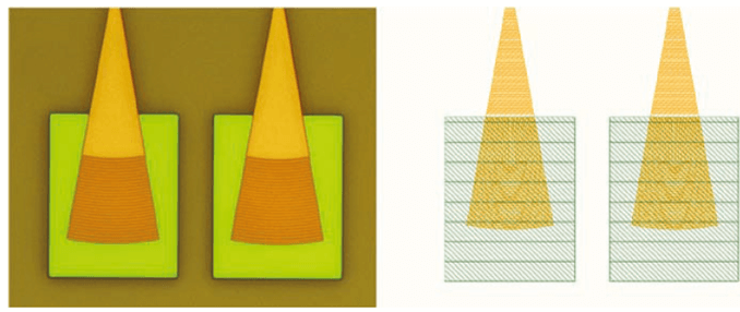
It is necessary to integrate materials with narrower bandgaps than Si as the detection (absorption) medium within the working wavelength range of silicon photonic chips. Germanium (Ge) can be epitaxially grown and absorbs light at communication wavelengths. While this is essential for compatibility with standard infrastructure, it is not strictly necessary for short-distance applications where both ends of the link can be defined without adhering to interoperability standards. Bonding III-V materials have also been used for photodetection. These materials are closely integrated or directly connected near Si waveguides, allowing guided light to enter the photodetector through evanescent or facet coupling, and the photodetector can have a small cross-section to reduce device capacitance and improve speed.
The latest technology level for Ge photodetectors, configured as photodiodes, achieves a bandwidth of 120 GHz and a responsivity of 0.8 A/W. At a frequency of 20 GHz, for a wavelength of 1550 nm, a responsivity of 1.05 A/W has been demonstrated, equivalent to 84% quantum efficiency. Figure 7 shows an example of a germanium photodetector. In photodetector devices estimated to have a quantum efficiency of 90% and a bandwidth of 40 GHz, an extremely low photodetector capacitance of 2.4 fF has been achieved.
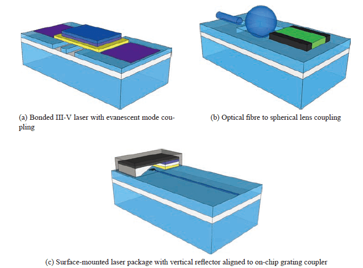
One of the primary challenges in silicon photonics platforms is the lack of on-chip light sources. Currently, the generation of silicon photonic chips relies on external laser coupling. Although edge couplers and grating couplers have improved coupling efficiency, the absence of on-chip light sources limits the potential applications of these chips.
To address the light source issue, several techniques have been proposed, which I’ll briefly discuss here. Hybrid silicon lasers have been developed by transferring III-V materials onto silicon wafers using bonding and epitaxial growth. However, these techniques face limitations due to the incompatibility of III-V materials with standard CMOS processes, as well as the high cost and low yield of bonding, along with the small available III/V wafer sizes. Ge (germanium), despite its limited light emission efficiency due to its indirect bandgap, has been proposed as a CMOS-compatible gain medium. The small (134 meV) difference between indirect and direct bandgaps can be overcome through strain engineering and heavy n-type doping. Electrically driven lasers using Ge as the gain medium have been validated on Si.
Currently, all market products adopt more conventional methods. These methods include non-on-chip light sources connected via optical fibers to silicon chips and lasers integrated within the same package as silicon photonic chips. These integration techniques, originating from the MEMS field, leverage micro-packaging technology, which is both cost-effective and highly mature.
Methods for Photonic-Electronic Integration
The integration of photonics and electronics is a crucial step in enhancing information processing system capabilities. It enables faster data transmission rates, lower power consumption, and more compact device designs, opening up significant new opportunities for system design. Integration methods typically fall into two categories: single-chip integration and multi-chip integration.
Single-Chip Integration: Single-chip integration involves manufacturing photonic and electronic components on the same substrate, typically using compatible materials and processes. This approach primarily aims to create seamless interfaces between light and electricity within a single chip.
Advantages:
Reduced Interconnect Losses: Placing photonic and electronic components close together minimizes signal losses associated with external chip connections.
Improved Performance: Tighter integration leads to faster data transmission speeds, as shorter signal paths reduce latency.
Smaller Footprint: Single-chip integration allows highly compact devices, particularly beneficial for space-constrained applications like data centers or handheld devices.
Lower Power Consumption: Eliminating the need for separate packaging and long-distance interconnects significantly reduces power requirements.
Challenges:
Material Compatibility: Finding materials that support both high-quality electronics and photonic functionality can be challenging, as they often require different properties.
Process Compatibility: Integrating diverse manufacturing processes for electronics and photonics on the same substrate without compromising the performance of any component is a complex task.
Complex Manufacturing: The high precision required for both electronic and photonic structures adds complexity and cost to manufacturing processes.
Multi-Chip Integration
This approach allows for greater flexibility in selecting materials and processes for each function. In multi-chip integration, electronic and photonic components come from different processes and are then assembled together, placed on a common package or substrate. Let’s now explore the bonding methods used between optoelectronic chips:
Direct Bonding: This technique involves direct physical contact and bonding of two planar surfaces, typically facilitated by molecular bonding forces, heat, and pressure. It offers simplicity and potentially very low-loss connections, but requires precise alignment and clean surfaces.
Fiber/Grating Coupling: In this scheme, optical fibers or fiber arrays are aligned and bonded to the edges or surfaces of photonic chips, allowing light to be coupled in and out of the chip. Gratings can also be used for vertical coupling, enhancing light transmission between the photonic chip and external fibers.
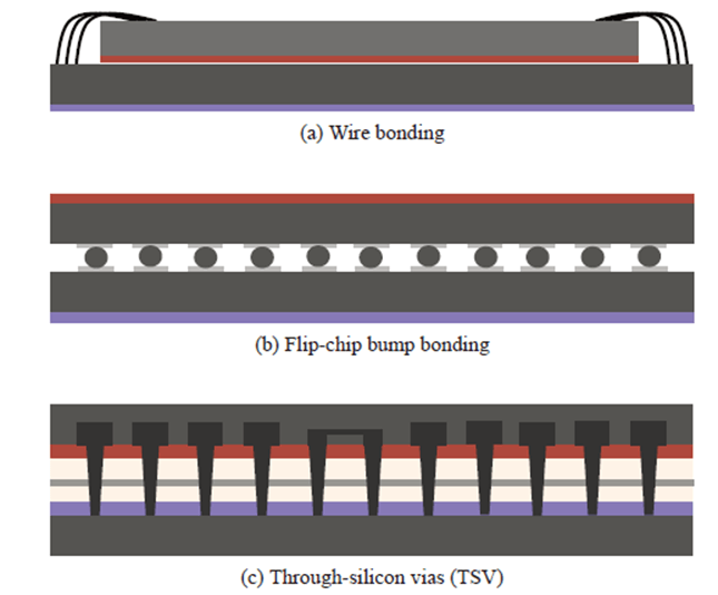
Silicon Through Vias (TSVs) and Microbumps: TSVs enable vertical interconnects through the silicon substrate, allowing chips to be stacked in three dimensions. Combined with microbumps, they facilitate electrical connections between electronic and photonic chips in stacked configurations, suitable for high-density integration.
Optical Interposer: An optical interposer is an independent substrate containing optical waveguides, serving as an intermediary for routing light signals between chips. It allows precise alignment and can integrate additional passive optical components, enhancing connection flexibility.
Hybrid Bonding: This advanced bonding technique combines direct bonding and microbump technology to achieve high-density electrical connections between chips and high-quality optical interfaces. It holds promise for high-performance optoelectronic co-integration.
Solder Bump Bonding: Similar to flip-chip bonding, solder bumps are used to create electrical connections. However, in the context of optoelectronic integration, special care must be taken to avoid heat-induced damage to photonic components and maintain optical alignment.
The benefits of these methods are significant. As the CMOS world continues to follow Moore’s Law improvements, it will be possible to rapidly adapt each generation of CMOS or Bi-CMOS to an inexpensive silicon photonics chip, reaping the benefits of optimal processes for both photonics and electronics. Since photonics typically doesn’t require manufacturing extremely small structures (typical critical dimensions are around 100 nanometers), and the devices are much larger compared to transistors, economic considerations will favor separate manufacturing of photonic devices in a dedicated process, decoupled from any advanced electronics required for the final product.
Advantages:
Flexibility: Independent use of different materials and processes to achieve optimal performance for electronic and photonic components.
Process Maturity: Leveraging mature manufacturing processes for each component can simplify production and reduce costs.
Easier Upgrades and Maintenance: Component separation allows easier replacement or upgrading of individual parts without affecting the entire system.
Challenges:
Interconnect Loss: External chip connections introduce additional signal loss, potentially requiring complex alignment procedures.
Increased Complexity and Size: Separate components necessitate additional packaging and interconnects, leading to larger dimensions and potentially higher costs.
Higher Power Consumption: Longer signal paths and additional packaging may increase power requirements compared to single-chip integration.
Conclusion
The choice between single-chip integration and multi-chip integration depends on specific application requirements, including performance goals, size constraints, cost considerations, and technological maturity. While more complex to manufacture, single-chip integration is advantageous for applications demanding extreme miniaturization, low power, and high-speed data transfer. Conversely, multi-chip integration offers greater design flexibility and leverages existing manufacturing capabilities, making it suitable for applications where these factors outweigh the benefits of tighter integration. Ongoing research explores hybrid approaches that combine elements of both strategies to optimize system performance while mitigating challenges associated with each method.
Related Products:
-
 NVIDIA MMS4X00-NM-FLT Compatible 800G Twin-port OSFP 2x400G Flat Top PAM4 1310nm 500m DOM Dual MTP/MPO-12 SMF Optical Transceiver Module
$1199.00
NVIDIA MMS4X00-NM-FLT Compatible 800G Twin-port OSFP 2x400G Flat Top PAM4 1310nm 500m DOM Dual MTP/MPO-12 SMF Optical Transceiver Module
$1199.00
-
NVIDIA MMA4Z00-NS-FLT Compatible 800Gb/s Twin-port OSFP 2x400G SR8 PAM4 850nm 100m DOM Dual MPO-12 MMF Optical Transceiver Module
$650.00
-
NVIDIA MMS4X00-NM Compatible 800Gb/s Twin-port OSFP 2x400G PAM4 1310nm 500m DOM Dual MTP/MPO-12 SMF Optical Transceiver Module
$900.00
-
NVIDIA MMA4Z00-NS Compatible 800Gb/s Twin-port OSFP 2x400G SR8 PAM4 850nm 100m DOM Dual MPO-12 MMF Optical Transceiver Module
$650.00
-
NVIDIA MMS1Z00-NS400 Compatible 400G NDR QSFP112 DR4 PAM4 1310nm 500m MPO-12 with FEC Optical Transceiver Module
$700.00
-
NVIDIA MMS4X00-NS400 Compatible 400G OSFP DR4 Flat Top PAM4 1310nm MTP/MPO-12 500m SMF FEC Optical Transceiver Module
$700.00
-
NVIDIA MMA1Z00-NS400 Compatible 400G QSFP112 VR4 PAM4 850nm 50m MTP/MPO-12 OM4 FEC Optical Transceiver Module
$550.00
-
NVIDIA MMA4Z00-NS400 Compatible 400G OSFP SR4 Flat Top PAM4 850nm 30m on OM3/50m on OM4 MTP/MPO-12 Multimode FEC Optical Transceiver Module
$550.00