Table of Contents
ToggleIntroduction
Amid the rapid development of artificial intelligence (AI) and machine learning (ML), the demand for faster, more efficient, and scalable computing infrastructure is growing rapidly. As we continue to push the boundaries of what’s possible with AI, new challenges in data transmission and processing emerge. Optical Computing Interconnect (OCI) technology has also emerged as a breakthrough technology that is expected to revolutionize the way we build and connect AI systems.
Challenge: Input/Output Bottlenecks in AI Infrastructure
As AI models become more complex and large, the amount of data that needs to be transmitted between computing nodes grows exponentially. Traditional electrical interconnects struggle to meet these demands, creating bottlenecks that limit the overall performance of AI systems.

Well-known challenges are now accelerated by AI
This diagram clearly shows how computing network interconnects have historically lagged behind the evolving bandwidth requirements of AI applications. As AI continues to advance, this gap is expected to widen further, creating an urgent need for new solutions.
Solution: Photoelectronic Integration and OCI
To address these challenges, researchers and engineers are turning to pshotoelectronic integration, specifically optical computing interconnect (OCI) technology. OCI uses light to transmit data, which has several key advantages over traditional electrical interconnects:
- Higher bandwidth
- Lower power consumption with lower density
- Lower latency
- Longer transmission distance
Application of OCI in AI Infrastructure
OCI technology has two main applications in AI infrastructure: computing fabric (AI/ML cluster) and resource decomposition.
Computing Fabric (AI/ML Cluster)
In AI/ML clusters, OCI can be used to connect CPU/GPU-based servers, either as node-to-node connections or in switched fabric configurations.
This application offers several advantages:
- It provides increased bandwidth for larger clusters
- Copper interconnects extend transmission distances
- Lower latency
- Reduced power consumption
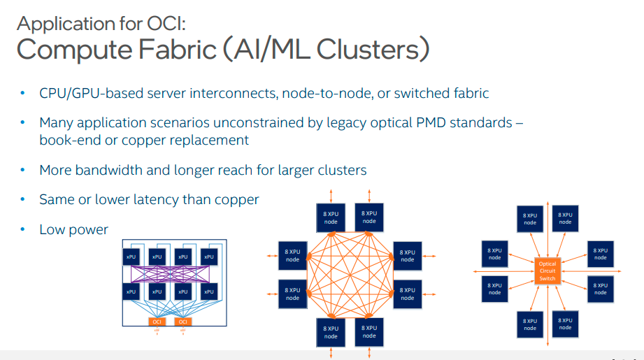
Application for OCI in AI/ML cluster computing Fabric
This diagram shows how OCI is used to connect multiple XPU (CPU/GPU) nodes in an AI/ML cluster, enabling high-bandwidth, low-latency communication between computing resources.
Resource breakdown
OCI also enables resource decomposition, allowing the creation of larger shared resource pools across multiple compute nodes. This approach offers several advantages:
- Free resources from packaging and slot constraints
- Improve resource utilization and efficiency
- Latency-sensitive connections
- High bandwidth density
- Low power consumption
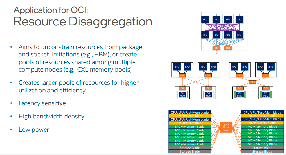
The application for OCI in resource disaggregation
This diagram depicts how OCI enables the decomposition of various compute resources such as CPU/XPU, memory, accelerators, and storage, allowing for more flexible and efficient utilization of these components in AI infrastructure.
Intel’s OCI approach
Intel is at the forefront of OCI development, leveraging its expertise in silicon-based photonics and advanced packaging to create scalable solutions for AI infrastructure.
Their approach focuses on three key areas:
- Integrate more photoelectronic functions on photoelectronic integrated chips (PICs)
- Integrate PIC with best-in-class electronic integrated circuit (EIC) using advanced packaging technology
- Tighter integration of optical chiplets with the host (XPU, switch)
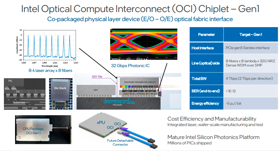
Intel’s OCI Chiplet-Gen1
This diagram illustrates Intel’s OCI Chiplet concept, tightly integrating the xPU (CPU or GPU) with the OCI module to enable high-bandwidth, low-latency optical communication directly from the compute unit.
OCI and the Future of AI Infrastructure
As AI continues to advance and the demand for more powerful computing power increases, OCI technology will play a key role in enabling the next generation of AI infrastructure. Intel’s OCI development roadmap includes:
- Expand number of wavelengths
- Increase line rate
- Expand the number of optical fibers
- Use polarization technology
These advances will enable continued improvements in bandwidth, power efficiency, and scalability, ultimately enabling more powerful and efficient AI systems.
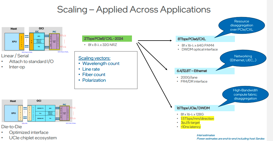
The Intel OCI scaling roadmap
This chart shows Intel’s grand plan for the expansion of OCI technology, which is expected to significantly increase bandwidth from 2Tbps PCIe5/CXL to 16Tbps UCIe/DWDM in future iterations.
In summary, OCI technology represents a significant advancement in solving the interconnect challenges of modern AI infrastructure. By leveraging the power of integrated photonics, OCI is expected to deliver the bandwidth, latency, and power efficiency required for next-generation AI and ML applications. As companies like Intel continue to invest and develop this technology, we can expect to see increasingly powerful and efficient AI systems that will push the possibilities of AI forward.
Specific implementation of OCI technology Intel has made significant progress in the implementation of OCI technology. Here are some key technical details:
Photonic Integrated Circuit (PIC)
Intel has developed a fully integrated 8Tbps PIC chip with the following features:
- Dense Wavelength Division Multiplexing (DWDM) Optical Interface
- 8 fiber pairs x 8 wavelengths x 64G, compliant with CW-WDM MSA standards
- 4Tbps throughput in each direction
- Standard single mode fiber output with low numerical aperture and V-groove for passive alignment
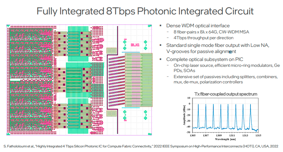
Intel’s 8Tbps photonic integrated circuit
This highly integrated PIC contains a complete optical subsystem, including an on-chip laser source, a high-efficiency micro-ring modulator, a germanium photodetector, and a semiconductor optical amplifier. This high level of integration not only improves performance but also reduces cost and power consumption.
Heterogeneous Integration
Intel uses wafer-level heterogeneous integration technology to integrate III-V materials (such as InP) with silicon-based optoelectronic devices. This approach has the following advantages:
- Performance: Minimizing coupling losses
- Reliability: Laser reliability < 0.1 FIT
- Manufacturability: Wafer level to known good die (KGD)
- Cost: No expensive laser backend required
- Scalability: high channel count, resource sharing
- Flexibility: multi-wavelength capability, backup
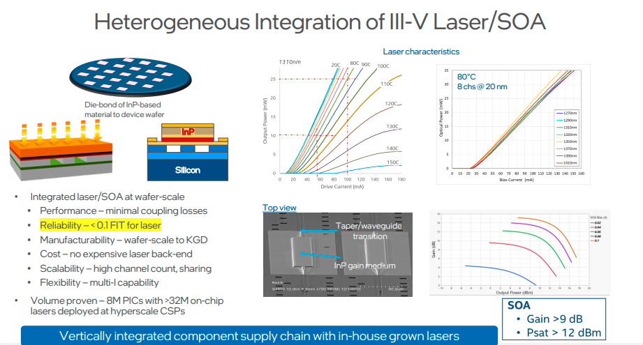
heterogeneous integration of III-V laser/SOA
This heterogeneous integration technology has been demonstrated in more than 8 million PICs deployed at hyperscale cloud service providers, containing more than 32 million on-chip lasers.
OCI Chiplet
Intel’s OCI Chiplet is a die stack that provides optical I/O using Intel’s silicon photonics technology and can be co-packaged with the xPU. The main parameters of the first generation OCI chiplet include:
- Host interface: PCIe gen5 SerDes interface
- Optical side: 8 fibers x 8 wavelengths x 32G NRZ, dense wavelength division multiplexing over single mode fiber
- Total bandwidth: 4 Tbps (2 Tbps each way)
- End-to-end bit error rate: < 1E-12
- Energy efficiency: ~5 pJ/bit
Intel’s concept CPU with co-packaged OCI demonstrated at OFC 2024 showed the practical application of this technology. The demonstration showed that in terms of optical links alone, OCI technology provides more than 3 times the power and 5 times the density improvement over pluggable modules.
Future Development of OCI Technology
Intel has a clear roadmap for the development of OCI technology, including the following key directions:
- Expansion of the number of wavelengths: from the current 8 wavelengths to 16 wavelengths or even more
- Increased line rate: From 32G NRZ to 64G PAM4, and may reach 128G or higher in the future.
- Increase in the number of optical fibers: Increase the number of optical fibers while maintaining miniaturization, thereby increasing the total bandwidth.
- Leveraging polarization technology: Further increase bandwidth density through polarization multiplexing.
These advances will enable OCI technology to support AI and high-performance computing applications with higher bandwidth, lower latency, and greater energy efficiency.
Conclusion
OCI technology represents a significant breakthrough in AI infrastructure interconnects. By leveraging the advantages of integrated optoelectronics, OCI delivers the high bandwidth, low latency, and high energy efficiency required for next-generation AI and ML applications. As companies like Intel continue to invest and develop this technology, we can expect to see more powerful and efficient AI systems emerge, driving continued progress in the field of artificial intelligence.
OCI technology not only solves the challenges facing current AI infrastructure, but also provides a scalable solution for future development. Through continuous technological innovation and industry collaboration, OCI has the potential to become a key technology supporting the next generation of AI and high-performance computing infrastructure.
This article introduces the principles, applications and development prospects of OCI technology in detail, hoping to provide readers with a comprehensive understanding of this emerging technology. As technology continues to advance, we can expect OCI to play an increasingly important role in advancing the fields of AI and high-performance computing.
