The current explosive growth of AI models and calculations requires parallel operations on multiple GPUs, which has led to an increase in the interface bandwidth between GPUs. NVIDIA is the most direct user in the AI optical module market. It has put forward several requirements and prospects for integrated photonics: low cost < $0.25/Gbps, low power consumption < 1.5pJ/b, long-distance transmission > 500m, single-fiber high bandwidth > 0.8Tbps, small size > 0.5Tbps/mm2, and high reliability < 100 FIT. The following figure is its architecture diagram for integrated photonics, which uses 3D packaging. Each IO uses optical transmission and the electrical chip is reversed on the optical chip, with optical chip, GPU, HBMs and switch packaged on the same interposer, communicating through the interposer.
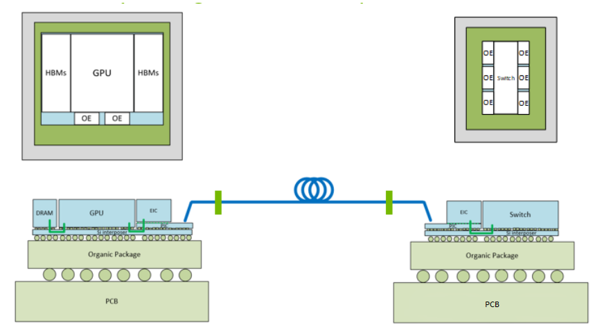
Architecture Diagram for Integrated Photonics
In such a high-density integrated system, it is more supportive of MRM-based DWDM links. It is mainly based on the following considerations: single-channel 25-50Gbps transmission can be achieved, single-chip power consumption is <1pJ/bit, the average single-channel area is as small as 50umx50um, and large capacity can be achieved through high-density integration.
.png)
The main challenges of MRM-based DWDM systems lie in silicon photonics device performance, multi-wavelength lasers, integrated packaging, thermal management and control.
- MRM
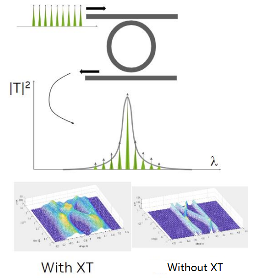
The first thing to solve in DWDM systems is channel crosstalk. The Lorentz filter spectrum has tails in other channels, while photodiodes and other components are broadband and have no wavelength selectivity. Therefore, in the system, crosstalk comes from the modulation influence of adjacent channels at the transmitting end, the adjacent channel crosstalk of demux at the receiving end, and multipath interference ISI caused by adjacent ring modulation. MRM usually requires balanced loss and modulation bandwidth. Low Q will not only increase the bandwidth, but also XT. Therefore, the effect can be reduced by increasing the channel spacing or using a higher order ring filter.
- Laser
Usually each optical fiber has 8-16 channels, which require corresponding wavelengths. The output power of each fiber-coupled optical laser is ~5mW. Taking into account coupling losses, passive device losses and power consumption, the efficiency is about 10%, corresponding to 2 pJ/b. Laser channel spacing is 100-200 GHz with ± 5-10% drift over temperature, which takes into account both low cost and low noise. There are currently the following types of lasers, and which one to adopt depends on the capabilities of each company.
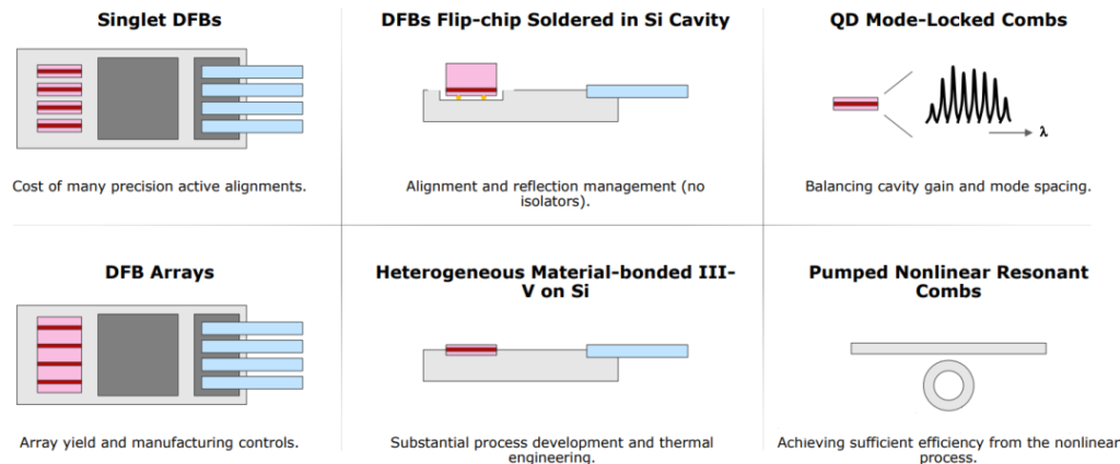
Forms of Laser
- 2.5D packaging
Coupled grating, large coupling tolerance, low spectral bandwidth, 1-2dB loss, usually 127-250um spacing, can be tested and packaged on chip.
End-face coupling, requiring higher coupling accuracy, high spectral bandwidth, and additional manufacturing aids (V-grooves, meta materials).
Both of the above solutions are acceptable, but they need to be mechanically robust. It is best to use independent EIC/PIC to achieve the best process. The EIC is on the PIC, and the PIC uses TSV to connect the EIC and interposer communication. The main thing is the thermal management of the entire structure.
- Thermal simulation
The device performance of silicon photonics chips is sensitive to heat, and ASIC and EIC chips are high heat generators. The figure below is a simulated diagram, where the ASIC power is evenly distributed on the chip, the EIC power is constant, and the heat flow temperature changes directly from the ASIC to the PIC and EIC. By adding plastic directly to the PIC and ASIC, good insulation can be achieved and the temperature rise will not exceed 10K. The temperature changes of the on-chip MRM and adjacent MRM through the monitoring film are 11 K and 0.7 K, respectively.
Related Products:
-
 NVIDIA MMS4X00-NM-FLT Compatible 800G Twin-port OSFP 2x400G Flat Top PAM4 1310nm 500m DOM Dual MTP/MPO-12 SMF Optical Transceiver Module
$1199.00
NVIDIA MMS4X00-NM-FLT Compatible 800G Twin-port OSFP 2x400G Flat Top PAM4 1310nm 500m DOM Dual MTP/MPO-12 SMF Optical Transceiver Module
$1199.00
-
NVIDIA MMA4Z00-NS-FLT Compatible 800Gb/s Twin-port OSFP 2x400G SR8 PAM4 850nm 100m DOM Dual MPO-12 MMF Optical Transceiver Module
$650.00
-
NVIDIA MMS4X00-NM Compatible 800Gb/s Twin-port OSFP 2x400G PAM4 1310nm 500m DOM Dual MTP/MPO-12 SMF Optical Transceiver Module
$900.00
-
NVIDIA MMA4Z00-NS Compatible 800Gb/s Twin-port OSFP 2x400G SR8 PAM4 850nm 100m DOM Dual MPO-12 MMF Optical Transceiver Module
$650.00
-
NVIDIA MMS1Z00-NS400 Compatible 400G NDR QSFP112 DR4 PAM4 1310nm 500m MPO-12 with FEC Optical Transceiver Module
$700.00
-
NVIDIA MMS4X00-NS400 Compatible 400G OSFP DR4 Flat Top PAM4 1310nm MTP/MPO-12 500m SMF FEC Optical Transceiver Module
$700.00
-
NVIDIA MMA1Z00-NS400 Compatible 400G QSFP112 VR4 PAM4 850nm 50m MTP/MPO-12 OM4 FEC Optical Transceiver Module
$550.00
-
NVIDIA MMA4Z00-NS400 Compatible 400G OSFP SR4 Flat Top PAM4 850nm 30m on OM3/50m on OM4 MTP/MPO-12 Multimode FEC Optical Transceiver Module
$550.00