Terminology and Basics
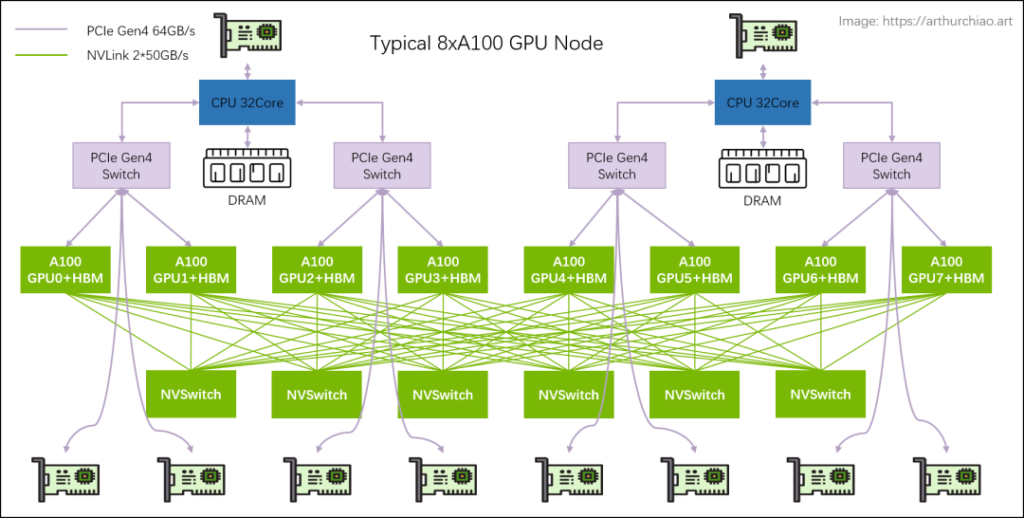
Large model training typically utilizes single-machine, 8-GPU hosts to form clusters. The models include 8*{A100, A800, H100, H800}. Below is the hardware topology of a typical 8*A100 GPU host:

PCIe Switch Chip
Devices such as CPUs, memory, storage (NVME), GPUs, and network cards that support PCIe can connect to the PCIe bus or a dedicated PCIe switch chip to achieve interconnectivity.
Currently, there are five generations of PCIe products, with the latest being Gen5.
NVLink
Definition
According to Wikipedia, NVLink is a wire-based serial multi-lane near-range communications link developed by Nvidia. Unlike PCI Express, a device can consist of multiple NVLinks, and devices use mesh networking to communicate instead of a central hub. The protocol was first announced in March 2014 and uses a proprietary high-speed signaling interconnect (NVHS).
In summary, NVLink is a high-speed interconnect method between different GPUs within the same host. It is a short-range communication link that ensures successful packet transmission, offers higher performance, and serves as a replacement for PCIe. It supports multiple lanes, with link bandwidth increasing linearly with the number of lanes. GPUs within the same node are interconnected via NVLink in a full-mesh manner (similar to spine-leaf architecture), utilizing NVIDIA’s proprietary technology.
Evolution: Generations 1/2/3/4
The main differences lie in the number of lanes per NVLink and the bandwidth per lane (the figures provided are bidirectional bandwidths):
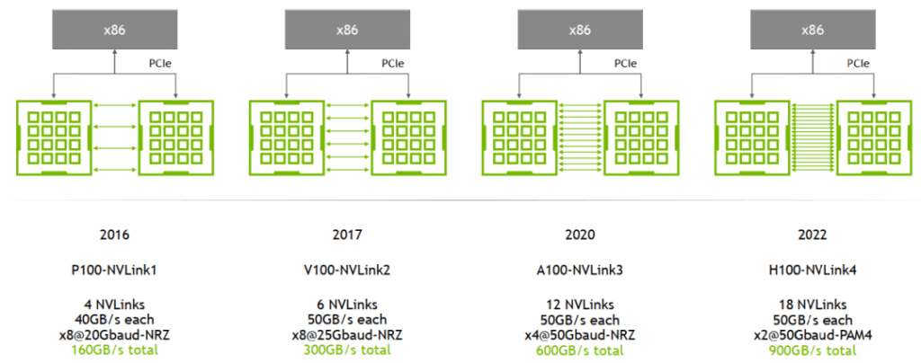
For example:
A100: 2 lanes/NVSwitch * 6 NVSwitch * 50GB/s/lane = 600GB/s bidirectional bandwidth (300GB/s unidirectional). Note: This is the total bandwidth from one GPU to all NVSwitches.
A800: Reduced by 4 lanes, resulting in 8 lanes * 50GB/s/lane = 400GB/s bidirectional bandwidth (200GB/s unidirectional).
Monitoring
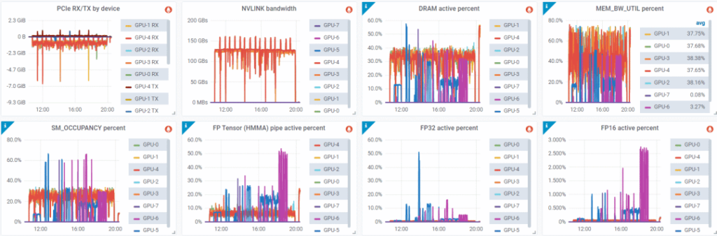
Real-time NVLink bandwidth can be collected based on DCGM metrics.
NVSwitch
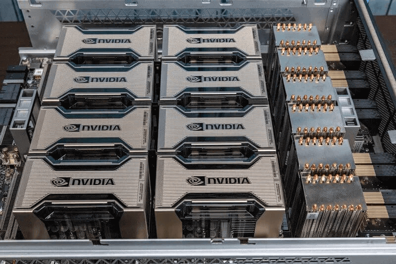
Refer to the diagram below for a typical 8*A100 GPU host hardware topology.
NVSwitch is an NVIDIA switch chip encapsulated within the GPU module, not an independent external switch.
Below is an image of an actual machine from Inspur. The eight boxes represent the eight A100 GPUs, and the six thick heat sinks on the right cover the NVSwitch chips:
NVLink Switch
Although NVSwitch sounds like a switch, it is actually a switch chip on the GPU module used to connect GPUs within the same host.
In 2022, NVIDIA released this chip as an actual switch called NVLink Switch, designed to connect GPU devices across hosts. The names can be easily confused.
HBM (High Bandwidth Memory)
Origin
Traditionally, GPU memory and regular memory (DDR) are mounted on the motherboard and connected to the processor (CPU, GPU) via PCIe. This creates a speed bottleneck at PCIe, with Gen4 offering 64GB/s and Gen5 offering 128GB/s. To overcome this, some GPU manufacturers (not just NVIDIA) stack multiple DDR chips and package them with the GPU. This way, each GPU can interact with its own memory without routing through the PCIe switch chip, significantly increasing speed. This “High Bandwidth Memory” is abbreviated as HBM. The HBM market is currently dominated by South Korean companies like SK Hynix and Samsung.
Evolution: HBM 1/2/2e/3/3e
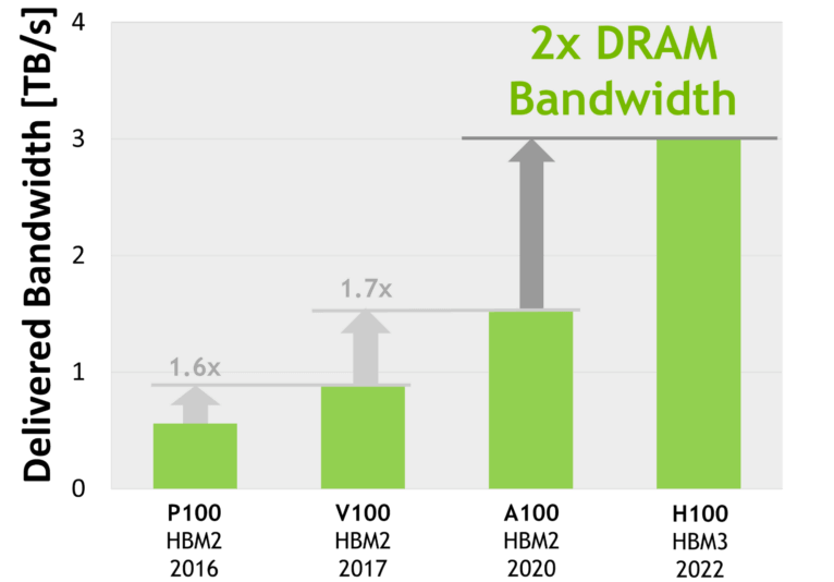
According to Wikipedia, the AMD MI300X uses a 192GB HBM3 configuration with a bandwidth of 5.2TB/s. HBM3e is an enhanced version of HBM3, with speeds ranging from 6.4GT/s to 8GT/s.
Bandwidth Units
The performance of large-scale GPU training is directly related to data transfer speeds. This involves various links, such as PCIe bandwidth, memory bandwidth, NVLink bandwidth, HBM bandwidth, and network bandwidth. Network bandwidth is typically expressed in bits per second (b/s) and usually refers to unidirectional (TX/RX). Other modules’ bandwidth is generally expressed in bytes per second (B/s) or transactions per second (T/s) and usually refers to total bidirectional bandwidth. It is important to distinguish and convert these units when comparing bandwidths.
Typical 8A100/8A800 Host
Host Topology: 2-2-4-6-8-8
- 2 CPUs (and their respective memory, NUMA)
- 2 storage network cards (for accessing distributed storage, in-band management, etc.)
- 4 PCIe Gen4 Switch chips
- 6 NVSwitch chips
- 8 GPUs
- 8 GPU-dedicated network cards

The following diagram provides a more detailed view:
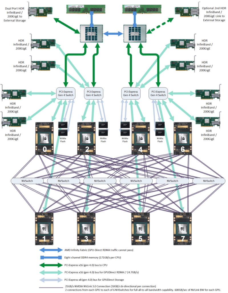
Storage Network Cards
These are directly connected to the CPU via PCIe. Their purposes include:
Reading and writing data from distributed storage, such as reading training data and writing checkpoints.
Normal node management, SSH, monitoring, etc.
The official recommendation is to use BF3 DPU, but as long as the bandwidth meets the requirements, any solution will work. For cost-effective networking, use RoCE; for the best performance, use IB.
NVSwitch Fabric: Intra-Node Full-Mesh
The 8 GPUs are connected in a full-mesh configuration via 6 NVSwitch chips, also known as NVSwitch fabric. Each link in the full-mesh has a bandwidth of n * bw-per-nvlink-lane:
For A100 using NVLink3, it is 50GB/s per lane, so each link in the full-mesh is 12*50GB/s = 600GB/s (bidirectional), with 300GB/s unidirectional.
For A800, which is a reduced version, 12 lanes are reduced to 8 lanes, so each link is 8*50GB/s = 400GB/s (bidirectional), with 200GB/s unidirectional.
Using nvidia-smi topo to View Topology
Below is the actual topology displayed by nvidia-smi on an 8*A800 machine (network cards are bonded in pairs, NIC 0~3 are bonded):
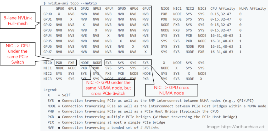
Between GPUs (top left area): All are NV8, indicating 8 NVLink connections.
Between NICs:
On the same CPU: NODE, indicating no need to cross NUMA but requires crossing PCIe switch chips.
On different CPUs: SYS, indicating the need to cross NUMA.
Between GPUs and NICs:
On the same CPU and under the same PCIe Switch chip: NODE, indicating only crossing PCIe switch chips.
On the same CPU but under different PCIe Switch chips: NODE, indicating crossing PCIe switch chips and PCIe Host Bridge.
On different CPUs: SYS, indicating crossing NUMA, PCIe switch chips, and the longest distance.
GPU Training Cluster Networking: IDC GPU Fabric
GPU Node Interconnection Architecture:
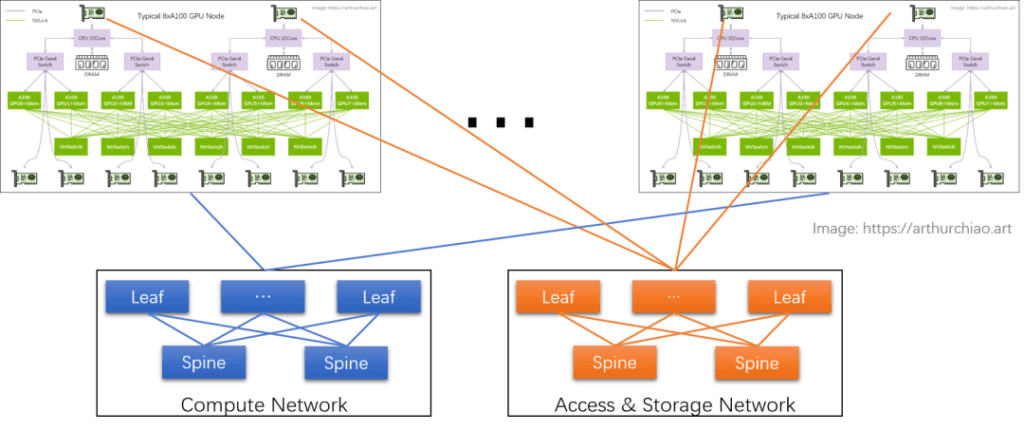
Compute Network:
The GPU network interface cards (NICs) are directly connected to the top-of-rack switches (leaf). These leaf switches are connected in a full-mesh topology to the spine switches, forming an inter-host GPU compute network. The purpose of this network is to facilitate data exchange between GPUs on different nodes. Each GPU is connected to its NIC through a PCIe switch chip: GPU <–> PCIe Switch <–> NIC.
Storage Network:
Two NICs directly connected to the CPU are linked to another network, primarily for data read/write operations and SSH management.
RoCE vs. InfiniBand:
Both the compute and storage networks require RDMA to achieve the high performance needed for AI. Currently, there are two RDMA options:
RoCEv2: Public cloud providers typically use this network for 8-GPU hosts, such as the CX6 with an 8*100Gbps configuration. It is relatively inexpensive while meeting performance requirements.
InfiniBand (IB): Offers over 20% better performance than RoCEv2 at the same NIC bandwidth but is twice as expensive.
Data Link Bandwidth Bottleneck Analysis:
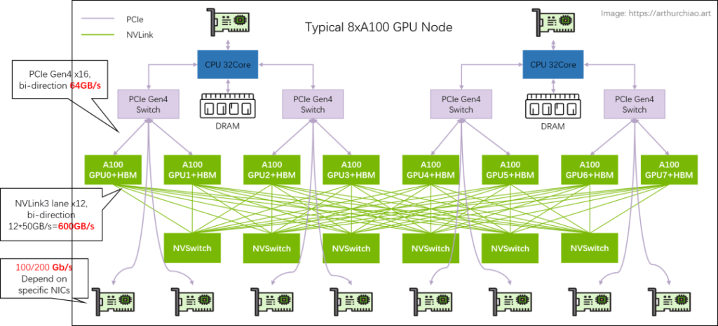
Key link bandwidths are indicated in the diagram:
Intra-host GPU communication: Utilizes NVLink with a bidirectional bandwidth of 600GB/s (300GB/s unidirectional).
Intra-host GPU to NIC communication: Uses PCIe Gen4 switch chips with a bidirectional bandwidth of 64GB/s (32GB/s unidirectional).
Inter-host GPU communication: Relies on NICs for data transmission. The mainstream bandwidth for domestic A100/A800 models is 100Gbps (12.5GB/s unidirectional), resulting in significantly lower performance compared to intra-host communication.
- 200Gbps (25GB/s): Approaches the unidirectional bandwidth of PCIe Gen4.
- 400Gbps (50GB/s): Exceeds the unidirectional bandwidth of PCIe Gen4.
Thus, using 400Gbps NICs in these models is not very effective, as 400Gbps requires PCIe Gen5 performance to be fully utilized.
Typical 8H100/8H800 Hosts
There are two types of GPU Board Form Factor:
- PCIe Gen5
- SXM5: Offers higher performance.
H100 Chip Layout:
The internal structure of an H100 GPU chip includes:
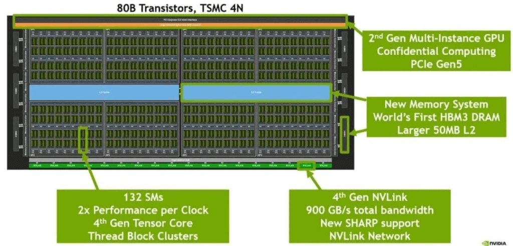
4nm process technology.
The bottom row consists of 18 Gen4 NVLink lanes with a total bidirectional bandwidth of 900GB/s (18 lanes * 25GB/s/lane).
The middle blue section is the L2 cache.
The sides contain HBM chips, which serve as the GPU memory.
Intra-host Hardware Topology:
Similar to the A100 8-GPU structure, with the following differences:
The number of NVSwitch chips has been reduced from 6 to 4.
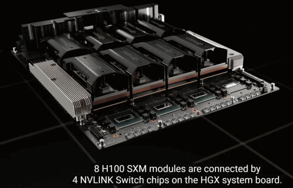
The connection to the CPU has been upgraded from PCIe Gen4 x16 to PCIe Gen5 x16, with a bidirectional bandwidth of 128GB/s.
Networking:
Similar to the A100, but the standard configuration has been upgraded to 400Gbps CX7 NICs. Otherwise, the bandwidth gap between the PCIe switch and NVLink/NVSwitch would be even larger.
Typical 4*L40S/8*L40S Hosts
The L40S is a new generation of cost-effective, multifunctional GPUs set to be released in 2023, positioned as a competitor to the A100. While it is not suitable for training large foundational models (as will be explained later), it is advertised as being capable of handling almost any other task.
Comparison of L40S and A100 Configurations and Features
One of the key features of the L40S is its short time-to-market, meaning the period from order to delivery is much shorter compared to the A100/A800/H800. This is due to both technical and non-technical reasons, such as: The removal of FP64 and NVLink.
The use of GDDR6 memory, which does not rely on HBM production capacity (and advanced packaging).
The lower cost is attributed to several factors, which will be detailed later.
The primary cost reduction likely comes from the GPU itself, due to the removal of certain modules and functions or the use of cheaper alternatives.
Savings in the overall system cost, such as the elimination of a layer of PCIe Gen4 switches. Compared to 4x/8x GPUs, the rest of the system components are almost negligible in cost.
Performance Comparison Between L40S and A100
Below is an official performance comparison:
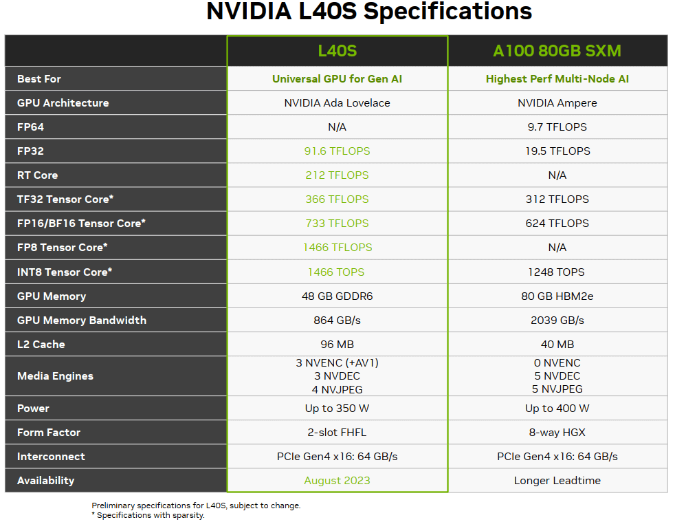
Performance: 1.2x to 2x (depending on the specific scenario).
Power consumption: Two L40S units consume roughly the same power as a single A100.
It is important to note that the official recommendation for L40S hosts is a single machine with 4 GPUs rather than 8 (the reasons for this will be explained later). Therefore, comparisons are generally made between two 4L40S units and a single 8A100 unit. Additionally, many performance improvements in various scenarios have a major prerequisite: the network must be a 200Gbps RoCE or IB network, which will be explained next.
L40S System Assembly
Recommended Architecture: 2-2-4
Compared to the A100’s 2-2-4-6-8-8 architecture, the officially recommended L40S GPU host architecture is 2-2-4. The physical topology of a single machine is as follows:
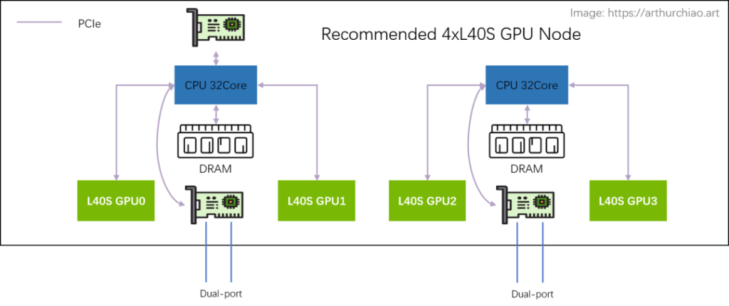
The most noticeable change is the removal of the PCIe switch chip between the CPU and GPU. Both the NIC and GPU are directly connected to the CPU’s built-in PCIe Gen4 x16 (64GB/s):
- 2 CPUs (NUMA)
- 2 dual-port CX7 NICs (each NIC 2*200Gbps)
- 4 L40S GPUs
Additionally, only one dual-port storage NIC is provided, directly connected to any one of the CPUs.
This configuration provides each GPU with an average network bandwidth of 200Gbps.
Non-Recommended Architecture: 2-2-8
As shown, compared to a single machine with 4 GPUs, a single machine with 8 GPUs requires the introduction of two PCIe Gen5 switch chips.
It is said that the current price of a single PCIe Gen5 switch chip is $10,000 (though this is unverified), and a single machine requires 2 chips, making it cost-ineffective.
There is only one manufacturer producing PCIe switches, with limited production capacity and long lead times.
The network bandwidth per GPU is halved.
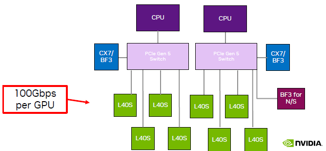
Networking
The official recommendation is for 4-GPU models, paired with 200Gbps RoCE/IB networking.
Analysis of Data Link Bandwidth Bottlenecks
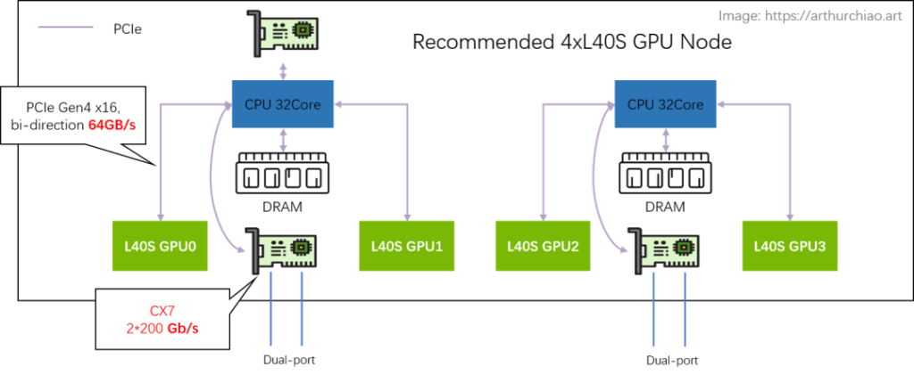
Using two L40S GPUs under the same CPU as an example, there are two possible link options:
- Direct CPU Processing:
Path: GPU0 <–PCIe–> CPU <–PCIe–> GPU1
Bandwidth: PCIe Gen4 x16 with a bidirectional bandwidth of 64GB/s (32GB/s unidirectional).
CPU Processing Bottleneck: To be determined.
- Bypassing CPU Processing:
Path: GPU0 <–PCIe–> NIC <– RoCE/IB Switch –> NIC <–PCIe–> GPU1
Bandwidth: PCIe Gen4 x16 with a bidirectional bandwidth of 64GB/s (32GB/s unidirectional).
Average Bandwidth per GPU: Each GPU has a unidirectional 200Gbps network port, equivalent to 25GB/s.
NCCL Support: The latest version of NCCL is being adapted for the L40S, with the default behavior routing data externally and back.
Although this method appears longer, it is reportedly faster than the first method, provided the NICs and switches are properly configured with a 200Gbps RoCE/IB network. In this network architecture, with sufficient bandwidth, the communication bandwidth and latency between any two GPUs are consistent, regardless of whether they are within the same machine or under the same CPU. This allows for horizontal scaling of the cluster.
Cost and Performance Considerations:
The cost of GPU machines is reduced. However, for tasks with lower network bandwidth requirements, the cost of NVLINK is effectively transferred to the network. Therefore, a 200Gbps network is essential to fully utilize the performance of multi-GPU training with the L40S.
Bandwidth Bottlenecks in Method Two:
The bandwidth bottleneck between GPUs within the same host is determined by the NIC speed. Even with the recommended 2*CX7 configuration:
- L40S: 200Gbps (unidirectional NIC speed)
- A100: 300GB/s (unidirectional NVLINK3) == 12x200Gbps
- A800: 200GB/s (unidirectional NVLINK3) == 8x200Gbps
It is evident that the inter-GPU bandwidth of the L40S is 12 times slower than the A100 NVLINK and 8 times slower than the A800 NVLINK, making it unsuitable for data-intensive foundational model training.
Testing Considerations:
As mentioned, even when testing a single 4-GPU L40S machine, a 200Gbps switch is required to achieve optimal inter-GPU performance.
Related Products:
-
 NVIDIA MMA4Z00-NS400 Compatible 400G OSFP SR4 Flat Top PAM4 850nm 30m on OM3/50m on OM4 MTP/MPO-12 Multimode FEC Optical Transceiver Module
$550.00
NVIDIA MMA4Z00-NS400 Compatible 400G OSFP SR4 Flat Top PAM4 850nm 30m on OM3/50m on OM4 MTP/MPO-12 Multimode FEC Optical Transceiver Module
$550.00
-
NVIDIA MMA4Z00-NS-FLT Compatible 800Gb/s Twin-port OSFP 2x400G SR8 PAM4 850nm 100m DOM Dual MPO-12 MMF Optical Transceiver Module
$650.00
-
NVIDIA MMA4Z00-NS Compatible 800Gb/s Twin-port OSFP 2x400G SR8 PAM4 850nm 100m DOM Dual MPO-12 MMF Optical Transceiver Module
$650.00
-
NVIDIA MMS4X00-NM Compatible 800Gb/s Twin-port OSFP 2x400G PAM4 1310nm 500m DOM Dual MTP/MPO-12 SMF Optical Transceiver Module
$900.00
-
NVIDIA MMS4X00-NM-FLT Compatible 800G Twin-port OSFP 2x400G Flat Top PAM4 1310nm 500m DOM Dual MTP/MPO-12 SMF Optical Transceiver Module
$1199.00
-
NVIDIA MMS4X00-NS400 Compatible 400G OSFP DR4 Flat Top PAM4 1310nm MTP/MPO-12 500m SMF FEC Optical Transceiver Module
$700.00
-
NVIDIA(Mellanox) MMA1T00-HS Compatible 200G Infiniband HDR QSFP56 SR4 850nm 100m MPO-12 APC OM3/OM4 FEC PAM4 Optical Transceiver Module
$139.00
-
NVIDIA MFP7E10-N010 Compatible 10m (33ft) 8 Fibers Low Insertion Loss Female to Female MPO Trunk Cable Polarity B APC to APC LSZH Multimode OM3 50/125
$47.00
-
NVIDIA MCP7Y00-N003-FLT Compatible 3m (10ft) 800G Twin-port OSFP to 2x400G Flat Top OSFP InfiniBand NDR Breakout DAC
$260.00
-
NVIDIA MCP7Y70-H002 Compatible 2m (7ft) 400G Twin-port 2x200G OSFP to 4x100G QSFP56 Passive Breakout Direct Attach Copper Cable
$155.00
-
NVIDIA MCA4J80-N003-FTF Compatible 3m (10ft) 800G Twin-port 2x400G OSFP to 2x400G OSFP InfiniBand NDR Active Copper Cable, Flat top on one end and Finned top on other
$600.00
-
NVIDIA MCP7Y10-N002 Compatible 2m (7ft) 800G InfiniBand NDR Twin-port OSFP to 2x400G QSFP112 Breakout DAC
$190.00