NVIDIA’s GPU technology undoubtedly shines brightly in today’s high-performance computing landscape. With the rapid development of artificial intelligence and machine learning, the demand for computational power continues to grow, making interconnectivity between GPUs increasingly crucial. Against this backdrop, NVIDIA introduced the NVLink protocol and the multi-GPU interconnect solution based on this technology: NV Switch.
This section delves into the development history, working principles, and key role of NV Switch in constructing high-performance server clusters, unveiling the mysterious aspects of this technology.
Why NV Switch is Needed
As individual GPU computational capabilities approach physical limits, collaborative work among multiple GPUs becomes an inevitable trend.
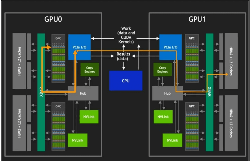
However, accessing other GPUs’ HBM2 memory requires traversing the PCIe interface. As shown in the diagram above, traditional PCIe interfaces have limitations in data transfer rates and bandwidth, often becoming performance bottlenecks for GPU communication. To overcome this limitation, NVIDIA developed NVLink technology, which provides ten times the bandwidth of PCIe. It allows eight GPUs within a single server to connect via point-to-point networks, forming a mixed-cubed mesh.
The core advantage of NVLink lies in bypassing traditional CPU allocation and scheduling mechanisms, enabling direct data exchange between GPUs. This design reduces data transfer latency and significantly enhances overall system throughput. Additionally, NVlink GPCs allow access to inter-card HBM2 memory data and enable interaction with HBM2 data within other GPUs.
In multi-GPU systems, NVLINK also serves as XBARs, acting as bridges between different GPUs, allowing data to flow freely. It cleverly avoids conflicts with the PCIe bus, allowing NVLink and PCIe to coexist as complementary solutions, collectively providing the necessary data transfer capabilities for the system.
NV Switch builds upon this foundation, supporting fully non-blocking fully interconnected GPU systems. By providing more NVLink interfaces without any intermediate GPU hops, it enables larger-scale GPU interconnectivity, resulting in more powerful computing clusters.
In NVIDIA’s technological evolution, the Pascal architecture first introduced NVLink, significantly improving GPU communication efficiency by creating a high-speed channel. However, the true leap occurred in the next-generation Volta architecture, accompanied by the birth of NVSwitch.
NVSwitch acts as an intelligent hub in the data transmission network, supporting additional NVLink links and allowing full interconnectivity among multiple GPUs. It greatly optimizes data exchange efficiency and flexibility.
As depicted in the figure, Volta architecture achieved 300GB/s communication between GPUs, while the Hopper architecture further advanced to 900GB/s. Behind this achievement lies the significant increase in NVLink link count, expanding from 6 in Volta to 18 in Hopper. It’s akin to adding overpasses and roundabouts to the original highway, enabling more efficient data flow between GPUs and providing robust support for high-performance computing and large-scale parallel processing.
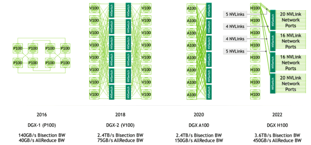
The diagram above illustrates the architecture of GPU interconnects in DGX servers. In DGX-1 P100, there are 8 GPU cards, each supporting 4 NVLink links that allow high-speed communication between GPUs. These GPUs are organized into two cube meshes, with each cube containing 4 GPUs (GPU 0~3 and GPU 4~7). Within each cube, GPUs can communicate directly via NVLink or through a PCIe switch. However, communication across cubes (e.g., between GPU 0 and GPU 4) requires indirect routing through other GPUs.
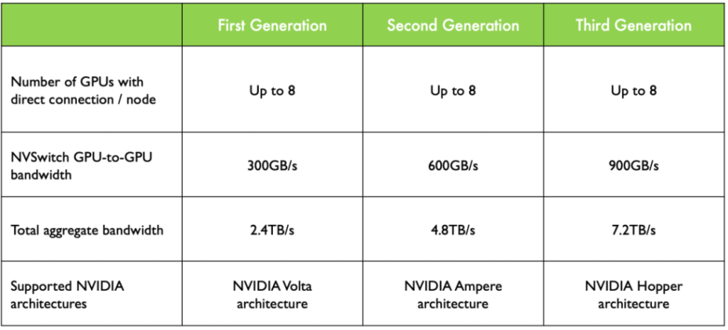
DGX-2 introduced NVIDIA’s first-generation NVSwitch technology, a significant advancement that enables more efficient communication between GPUs. In the Volta architecture, each GPU card supports 6 NVLink links (instead of 4). Additionally, by incorporating 6 NVSwitches, DGX-2 interconnects all GPUs in the server, allowing simultaneous communication between 8 pairs of GPUs without intermediate hops. This direct high-speed communication greatly enhances data transfer efficiency and overall computational performance.
DGX-A100 utilizes second-generation NVSwitch technology. Compared to the first generation, the second-generation NVSwitch provides higher communication bandwidth and lower latency. In the A100 architecture, each GPU card supports 12 NVLink (third-generation) links, and 6 NVSwitches create a fully connected network topology. Although the standard DGX A100 configuration includes only 8 GPU cards, the system can be expanded to support more A100 GPUs and NVSwitches for larger-scale supercomputing.
DGX-H100 employs third-generation NVSwitch and fourth-generation NVLink technologies. Each GPU card supports 18 NVLink links. In the H100 architecture, 4 NVSwitches are introduced, using a layered topology: each card connects to the first NVSwitch with 5 links, the second NVSwitch with 4 links, the third NVSwitch with 4 links, and the fourth NVSwitch with 5 links. This results in a total of 72 NVLinks providing 3.6 TB/s bidirectional NVLink network bandwidth, a 1.5x improvement over the previous generation.
The original NVSwitch design aimed to create a fully unblocked, fully interconnected GPU system for large-scale parallel processing. In the first generation, NVSwitch supported 18 interfaces, allowing up to 16 GPUs to be fully interconnected for efficient data sharing and communication.
As shown in the V100 architecture diagram, each GPU has 6 NVLink channels that connect to NVSwitch, forming a high-bandwidth communication network. In the DGX-2 system, 8 V100 GPUs are connected to 6 NVSwitches via these NVLink channels, creating a powerful backbone.
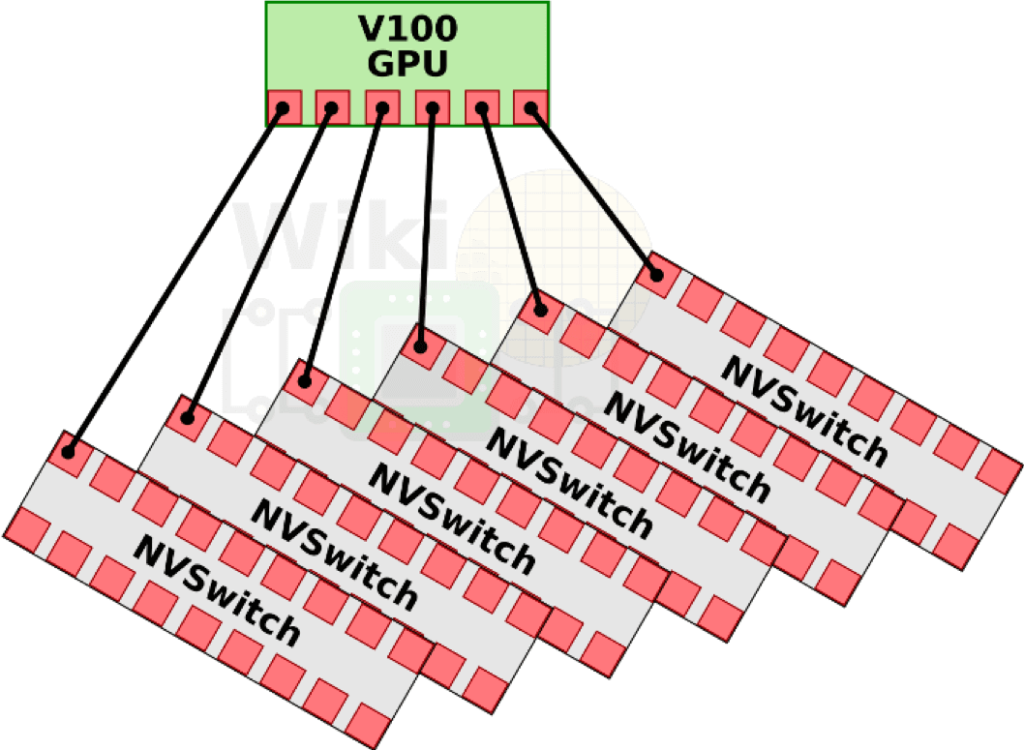
As shown in the diagram above, in the V100 architecture, each GPU has 6 NVLink channels that can connect to NVSwitch, forming a high-bandwidth communication network. In the DGX-2 system, 8 V100 GPUs are connected to 6 NVSwitches via these NVLink channels, creating a powerful backbone.
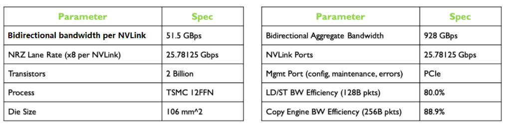
The first-generation NVSwitch supports NVLink 2.0 technology, with each interface providing dual channels and up to 50 GB/s bandwidth. This means that through NVSwitch, the entire system achieves an impressive total bandwidth of 900 GB/s, significantly enhancing data transfer rates and computational efficiency.
Furthermore, NVSwitch is manufactured using TSMC’s 12nm FinFET FFN process, allowing it to operate at 100W power while integrating up to 200 million transistors.
Regarding circuit I/O and packaging, NVSwitch is packaged in a large BGA chip with 1940 pins, of which 576 are specifically dedicated to supporting 18 NVLink links. The remaining pins handle power and various I/O interfaces, including x4 PCIe management ports, I2C, GPIO, providing flexible management and expansion capabilities for the system.
The specific parameters are shown in the table below:
NVLink bidirectional BW Up to 50 GB/s
Actual utilization Up to 80%
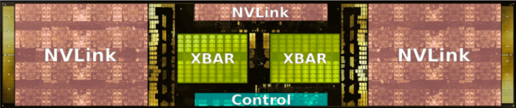
NV Switch Block
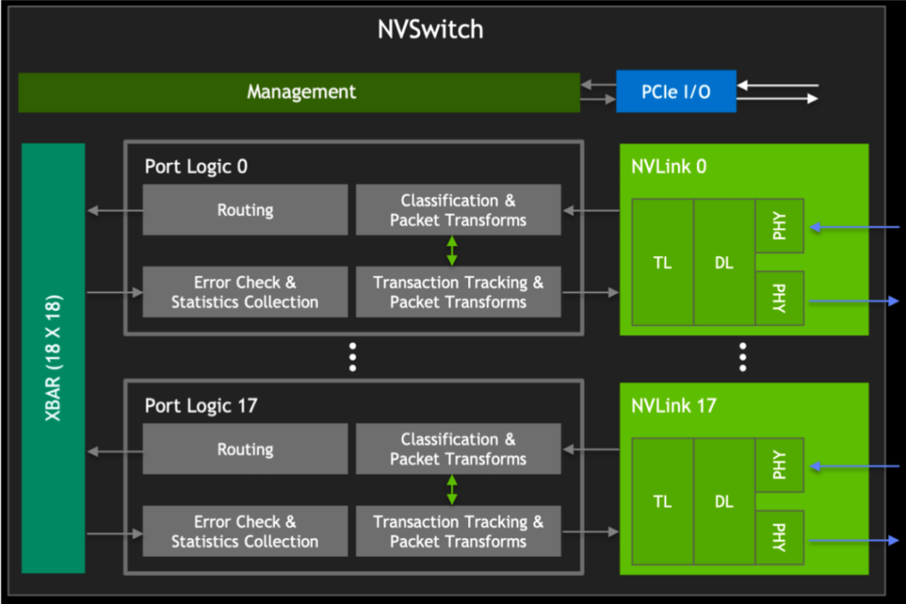
The initial NVSwitch block, as depicted, includes the GPU XBAR on the left. It is a highly specialized bridging device designed for NVLink interconnect environments, allowing data packets to flow and exchange between multiple GPUs while presenting externally as a single GPU. Through GPU XBAR, client applications can leverage the collective performance of multiple GPUs, reducing the complexity of managing GPU-to-GPU communication on the client side.
Additionally, GPU XBAR utilizes buffer technology based on static random-access memory (SRAM) to achieve non-blocking data transfer. This buffering mechanism ensures continuity and efficiency even under high loads.
Starting from the V100 GPU, NVIDIA reused the NVLink IP blocks and XBAR design, ensuring compatibility between different generations of products and enabling continuous iteration and optimization of NVLink technology while reducing development costs and time.
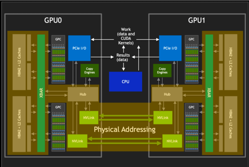
The diagram also illustrates how NVSwitch and GPUs distribute and transfer data across the entire GPU. In programming, developers typically deal with virtual addresses managed and abstracted by the operating system, providing independent address spaces for different programs. However, data is physically stored using physical addresses in memory. These physical addresses directly point to specific locations in memory, forming the foundation for data access. When transmitting data via NVLink, as shown in the diagram, physical addresses are used instead of virtual addresses. This choice accelerates data indexing and access speed.
NVSwitch, as the bridging device for NVLink, not only provides a high-bandwidth communication path but also manages complex routing and buffering mechanisms to ensure data packets are transmitted accurately and swiftly to their destination based on the correct physical address. Using physical addresses for NVLink communication reduces the need for address translation on the target GPU, thereby lowering latency and improving data transfer rates. This is crucial for high-performance computing and AI applications that require rapid processing of large amounts of data.
NVSwitch: Simplification Principles and Features
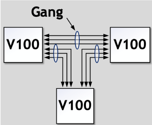
In configurations without NVSwitch, direct GPU-to-GPU connections typically involve aggregating NVLinks into multiple groups (referred to as “Gangs”). In this setup, multiple GPUs communicate via shared NVLink links. However, a limitation of this approach is that the maximum bandwidth between any two GPUs is constrained by the NVLink quantity and bandwidth within their respective Gangs.
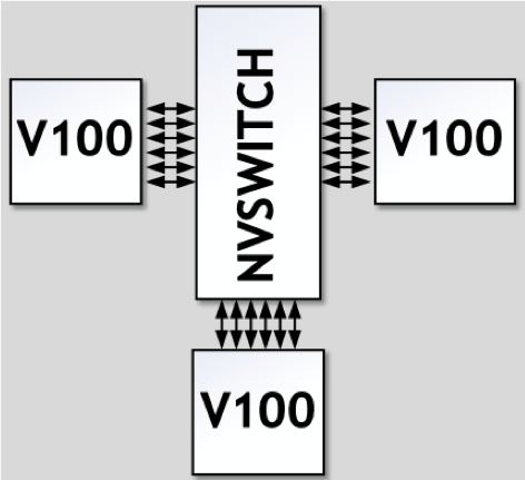
The Introduction of NVSwitch and Its Improvements NVIDIA’s NVSwitch technology revolutionizes communication between GPUs. As a high-speed switch, NVSwitch allows data interaction across all links.
In the NVSwitch architecture, any pair of GPUs can directly interconnect, and as long as the total bandwidth of six NVLinks is not exceeded, individual GPU traffic achieves non-blocking transmission. This means that the fully interconnected architecture supported by NVSwitch allows easy system scalability to accommodate more GPUs without sacrificing performance. Each GPU can leverage the high bandwidth provided by NVLink for rapid data exchange.
Advantages and Features of NVSwitch in Multi-GPU Interconnect:
Scalability and Expandability: The introduction of NVSwitch significantly enhances the scalability of GPU clusters. By simply adding more NVSwitches, the system can seamlessly support additional GPUs, expanding computational capacity.
Efficient System Construction: For example, eight GPUs can be efficiently interconnected using three NVSwitches. This design allows data to flow freely across all GPU links, maximizing flexibility and efficiency in data circulation.
Bidirectional Bandwidth Utilization: In this configuration, any GPU pair can utilize the full 300 GBps bidirectional bandwidth for communication. Each GPU achieves high-speed, low-latency data transfer, greatly enhancing computational task processing speed.
Non-Blocking Communication: The crossbar switch (XBAR) within NVSwitch provides a unique path from point A to point B for data transmission. This design ensures non-blocking and interference-free communication, further improving data transfer reliability and overall system performance.
Optimized Network Topology: NVSwitch supports network topology structures that offer optimized solutions for building large-scale GPU clusters. System designers can flexibly configure GPU-to-GPU connections based on specific computational requirements.
Third-Generation NVSwitch
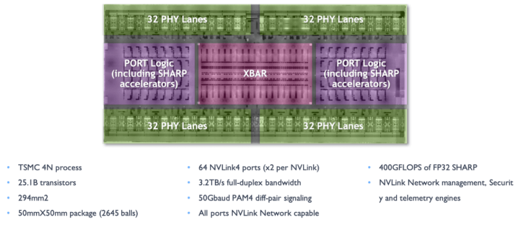
As depicted in the diagram, the third-generation NVSwitch is manufactured using TSMC’s 4N process. Despite having a large number of transistors and high bandwidth, it maintains relatively low power consumption. It provides 64 NVLink 4 link ports, enabling the construction of complex networks containing numerous GPUs while maintaining high-speed communication between each GPU. Additionally, it supports bidirectional bandwidth of 3.2 TB/s, significantly enhancing data transfer rates and making large-scale parallel processing of datasets more efficient.
Beyond connecting multiple GPU cards within a server, the third-generation NVSwitch can also extend to connect GPU servers externally, forming complete high-speed GPU clusters. A physical switch composed of third-generation NVSwitch chips can create clusters with up to 256 H100 GPUs, providing a total bandwidth of 57.6 TB/s.
Regarding signal technology, it adopts 50 Gbaud PAM4 signaling, with each differential pair providing 100 Gbps bandwidth, maintaining high-speed transmission and low latency.
NVSwitch integrates NVIDIA SHARP technology, including operations like all_gather, reduce_scatter, and broadcast atomics, accelerating cluster communication and further enhancing performance. NVSwitch 3.0’s physical electrical interface is compatible with 400 Gbps Ethernet and InfiniBand, ensuring interoperability with existing network technologies.
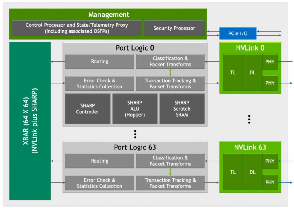
NVIDIA’s third-generation NVSwitch introduces several innovative features. The inclusion of the new SHARP module and NVLink module significantly improves efficient communication and data processing between GPUs, as shown in the diagram.
New SHARP Module
The newly introduced SHARP module acts as an intelligent conductor, leading a symphony of data with its powerful processing capabilities. It supports various operators, from logical to arithmetic operations, and is compatible with multiple data formats such as FP16 and BF16, providing robust support for AI and machine learning workloads. The SHARP controller’s design allows parallel management of up to 128 SHARP groups, akin to a multitasking thousand-armed deity, greatly enhancing data parallel processing efficiency.
The crossbar switch (XBAR) within NVSwitch, meticulously adjusted and optimized, perfectly matches the data transfer requirements of the SHARP module. This collaborative design ensures efficient and low-latency data transmission between GPUs, propelling the system’s overall performance like a galloping steed.
New NVLink Module
The integrated new NVLink module not only provides additional security protection for data and chips, acting as a robust shield against unauthorized access and potential data leaks, but also enhances data security. The introduction of port partitioning, like a strategic chess move, isolates different ports into separate NVLink networks, providing greater flexibility for logical resource partitioning across different networks and optimizing multitasking capabilities.
Support for the next-generation Octal Small Formfactor Pluggable (OSFP) cables ensures a solid foundation for future network expansion. These cables offer higher data transfer rates and lower signal attenuation, making them suitable for long-distance high-speed communication and enabling limitless possibilities for network scalability.
The new NVLink module also extends telemetry capabilities, allowing system administrators to precisely monitor and optimize network performance, ensuring stable system operation. Integrated forward error correction (FEC) technology acts as a vigilant guardian, enhancing data transmission reliability, especially in the face of signal attenuation or interference, guaranteeing data integrity and accuracy.
Comparison of InfiniBand (IB) and NVLink Networks for H100 GPUs
When H100 GPUs utilize NVLink networking, how much faster are they compared to A100 GPUs with IB networking? Let’s compare the bandwidth between DGX A100 256 POD and DGX H100 256 POD:
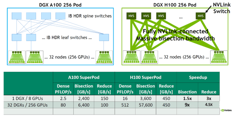
DGX A100 Internal Bandwidth:
Each DGX A100: 8/2 * 600 GB/s = 2400 GB/s
Across 32 DGX A100s (256 A100 GPUs), assuming 8x 200Gbps HDR NICs per server and a TOR switch convergence ratio of 4:1:
Total bandwidth = 256/2/4 * 200 GB/s = 6400 GB/s
DGX H100 Internal Bandwidth:
Each DGX H100: 8/2 * 900 GB/s = 3600 GB/s
Across 32 DGX H100s (256 H100 GPUs), with a convergence ratio of 2:1:
Total bandwidth = 256/2/2 * 900 GB/s = 57600 GB/s
Compared to DGX A100, a single DGX H100 provides a 1.5x increase in bandwidth and a 3x increase in bidirectional bandwidth. Using 32 DGX H100s, the per-lane bandwidth can be improved by 9x, and bidirectional bandwidth can be enhanced by 4.5x.
Summary
In today’s data-driven era, the demand for high-performance computing continues to push technological boundaries. NVIDIA’s NVSwitch technology, serving as the communication bridge between GPUs, plays a critical role in building efficient compute clusters. From the inception of the first NVSwitch to the innovations in the third generation, NVIDIA’s relentless pursuit of computational efficiency is evident. NVSwitch not only enhances data transfer bandwidth and speed but also strengthens data processing capabilities and system security through SHARP and NVLink modules. Its presence enables multi-GPU systems to collaborate more efficiently, providing robust support for fields like artificial intelligence, machine learning, and big data analytics. As technology advances, NVSwitch will remain pivotal in the high-performance computing landscape, symbolizing NVIDIA’s innovation and driving industry progress. Guided by NVSwitch, we anticipate a smarter, more efficient, and interconnected future.
Related Products:
-
 NVIDIA MMA4Z00-NS400 Compatible 400G OSFP SR4 Flat Top PAM4 850nm 30m on OM3/50m on OM4 MTP/MPO-12 Multimode FEC Optical Transceiver Module
$550.00
NVIDIA MMA4Z00-NS400 Compatible 400G OSFP SR4 Flat Top PAM4 850nm 30m on OM3/50m on OM4 MTP/MPO-12 Multimode FEC Optical Transceiver Module
$550.00
-
NVIDIA MMA4Z00-NS-FLT Compatible 800Gb/s Twin-port OSFP 2x400G SR8 PAM4 850nm 100m DOM Dual MPO-12 MMF Optical Transceiver Module
$650.00
-
NVIDIA MMA4Z00-NS Compatible 800Gb/s Twin-port OSFP 2x400G SR8 PAM4 850nm 100m DOM Dual MPO-12 MMF Optical Transceiver Module
$650.00
-
NVIDIA MMS4X00-NM Compatible 800Gb/s Twin-port OSFP 2x400G PAM4 1310nm 500m DOM Dual MTP/MPO-12 SMF Optical Transceiver Module
$900.00
-
NVIDIA MMS4X00-NM-FLT Compatible 800G Twin-port OSFP 2x400G Flat Top PAM4 1310nm 500m DOM Dual MTP/MPO-12 SMF Optical Transceiver Module
$1199.00
-
NVIDIA MMS4X00-NS400 Compatible 400G OSFP DR4 Flat Top PAM4 1310nm MTP/MPO-12 500m SMF FEC Optical Transceiver Module
$700.00
-
NVIDIA(Mellanox) MMA1T00-HS Compatible 200G Infiniband HDR QSFP56 SR4 850nm 100m MPO-12 APC OM3/OM4 FEC PAM4 Optical Transceiver Module
$139.00
-
NVIDIA MFP7E10-N010 Compatible 10m (33ft) 8 Fibers Low Insertion Loss Female to Female MPO Trunk Cable Polarity B APC to APC LSZH Multimode OM3 50/125
$47.00
-
NVIDIA MCP7Y00-N003-FLT Compatible 3m (10ft) 800G Twin-port OSFP to 2x400G Flat Top OSFP InfiniBand NDR Breakout DAC
$260.00
-
NVIDIA MCP7Y70-H002 Compatible 2m (7ft) 400G Twin-port 2x200G OSFP to 4x100G QSFP56 Passive Breakout Direct Attach Copper Cable
$155.00
-
NVIDIA MCA4J80-N003-FTF Compatible 3m (10ft) 800G Twin-port 2x400G OSFP to 2x400G OSFP InfiniBand NDR Active Copper Cable, Flat top on one end and Finned top on other
$600.00
-
NVIDIA MCP7Y10-N002 Compatible 2m (7ft) 800G InfiniBand NDR Twin-port OSFP to 2x400G QSFP112 Breakout DAC
$190.00