
In 2012, communication between two boards was achieved over optical fiber using the PCIE protocol. The advantages of doing so are: the reserved optical port allows the two devices to be physically separated, and the reserved optical interface and memory are compatible with and can be accessed by each other. As shown in the figure below, it shows the actual picture and physical block diagram of the four-way PCIE over fiber. The card is based on a PLX switch (PEX8609) that routes the upstream ports (x4 lanes) to the PCI connectors. The downstream ports are configured by the FPGA (Xilinx Spardan3AN) in two modes: four single-channel ports or one quad-channel port.
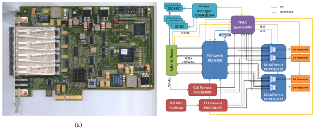
Two modes of FPGA
The lower left figure is a measured eye diagram of a 2.5 Gbps demonstration link based on PCI Express, which meets the PCIE GEN2 transmission rate. The article focuses more on improving the proton radiation tolerance test of Intel transceivers to ensure PCI Express compatibility meets the 5·10^11 p/cm2 requirement. The CMS experiment is shown in the figure on the right.
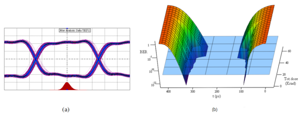
2.5 Gbps demonstration link based on PCI Express
According to an article published by the Polytechnic University of Milan in Italy in 2018, the figure below is a performance test diagram of a fiber optic link using PCIe Gen3. It has developed a small PCIE adapter card module equipped with an SFP+ interface and a small rack module with 4 PCIe slots. A host server PC contains a PCIe card (AERIAL1) with a 1310nm SFP+ commercial transceiver for 10G Ethernet applications. The card is connected to another PCIe card (AERIAL2) via an SMF link, both can be connected to the internet via Ethernet cards. A 90/10 splitter is added to the optical fiber link, and the split optical signal is received by the PD and then by a digital sampling oscilloscope (DSO) to evaluate the transmission performance.
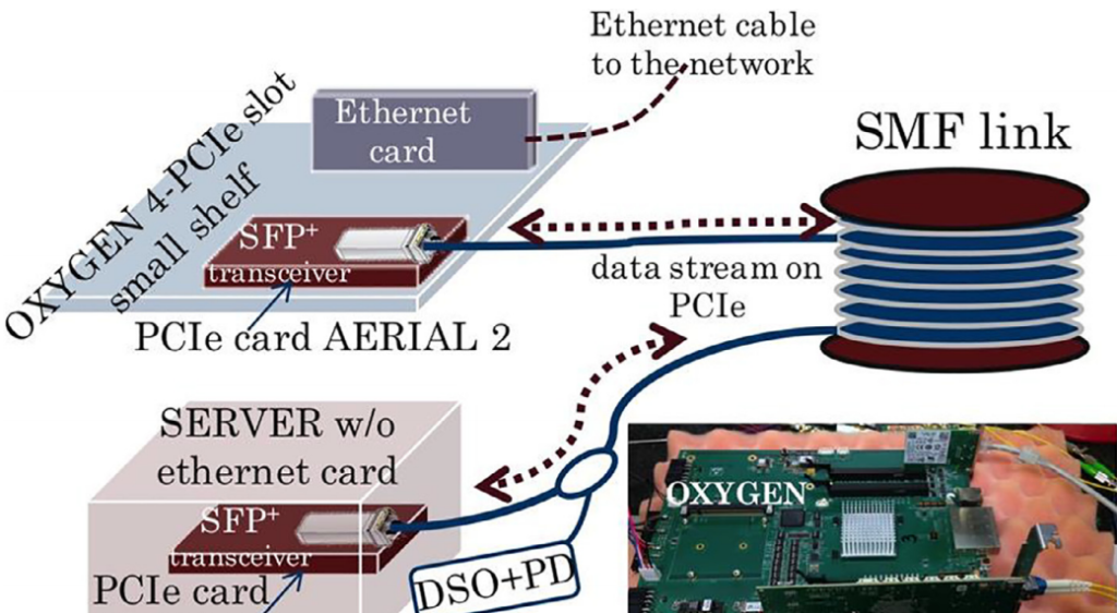
Performance Test Diagram of a Fiber Optic Link Using PCIe Gen3
The test results are shown in the figure below. The transmission rate is 8 Gb/s, the bit error rate performance after B2B 2^31-1 PRBS and SMF has no obvious transmission cost. Figure b shows eye diagram of optical PCIe Gen3 transmission.
Eye Diagram of Optical PCIe Gen3 Transmission
The figure below is a fiber optic link diagram for PCIE GEN4 with a tested fiber length of 2km and 10km. The BER is tested by changing the received power through VOA.
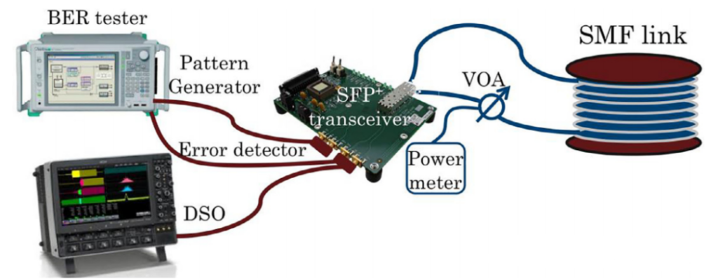
PCIE GEN4 Fiber Link Diagram
The figure below is the BER curve of the 2^31-1PRBS test at a transmission rate of 16 Gb/s. Its rate meets PCIE GEN4. It can be seen that for back-to-back (b2b), there is no obvious deterioration in power penalty of the optical fiber link.
BER curve of 2^31-1PRBS test at 16 Gb/s transmission rate
In fact, it can be seen here that in PCIE GEN2-GEN4, there is no obvious bottleneck in the transmission rate, and the traditional SFP module is still used. At this time, with the optical port only used as a transmission interface, PCIE over fiber does not have much advantage, but appears very bulky.
Ayar Labs divides shortline bandwidth density by energy efficiency to reflect the ability of different solutions to output data externally. As shown in the figure below, the horizontal axis is the signal transmission distance and the vertical axis is the FOM1 value. The picture includes electrical interconnection standards such as UCle, NVlink, and PCIe. Several points can be seen:
1. At the board level, as the transmission rate and latency requirements increase, the initial pluggable will develop towards CPO, especially for PCIE GEN5 and PCIE GEN6, the transmission rate reaches 32G and 64G, and the CPO packaging form will bring huge advantages to optical transceivers. If it develops further, it will move towards OIO, that is, a chip-based optical interconnect solution that is integrated in the same package as the computing chip (CPU, GPU, XPU), with bandwidth density, energy cost and latency comparable to electrical interconnects within the package.
2. The FOM1 value of Optical IO is comparable to that of electrical interconnection standards, but the transmission distance far exceeds them. The FOM1 value of CPO is one order of magnitude smaller than that of Optical IO. OIO will cover slave devices/boards/systems, which is the ultimate solution.
3. Inside the device, it will eventually develop towards UCIE, that is, chip-to-chip interconnection.
Signal transmission distance and FOM1 value
The image below shows Ayar Labs’ OIO, with four TeraPHY™ optical I/O chips in the same package as the main system-on-chip (SoC). It can achieve 16Tbps bidirectional transmission at an energy cost of <5 pJ/b in a typical size computing package (50mm x 50mm). The chips are compliant with the Universal Chiplet Interconnect Express™ (UCIe) standard and NVLink-C2C form.
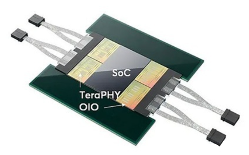
Ayar Labs’ OIO
Universal Chiplet Interconnect Express (UCIe)® is an open industry interconnect standard that enables package-level interconnection between chiplets, with the advantages of high bandwidth, low latency, and cost-effectiveness. Using 2.5D or 3D packaging, the core processor, memory and IO controller are packaged together to reduce the die area and thus improve performance.
The following figure summarizes the key performance metrics of the two packaging options. Several characteristics can be seen:
1. The pitch spacing continues to decrease to 25um, and the bandwidth density will increase to 3.24 times. Even at 45um, the bandwidth density is approximately 20 times that of the most efficient PCIe SERDES currently achievable.
2. The current ~10pJ/b energy efficiency of PCIe’s PHY can also be reduced to 1/20 through a UCIe-based design.
3. UCIe enables faster switching times in the power-bandwidth consumption curve, saving 90+% of energy.
In summary, PCIE over fiber is currently similar to a pluggable form and it uses light as the interface transmission medium. In the future, as bandwidth and latency requirements increase, it will develop towards CPO and OIO forms. At this time, core master control chips such as XPU are interconnected through UCIE, and boards communicate through OIO, which is the form that major manufacturers dream of.
Related Products:
-
 NVIDIA MMA4Z00-NS400 Compatible 400G OSFP SR4 Flat Top PAM4 850nm 30m on OM3/50m on OM4 MTP/MPO-12 Multimode FEC Optical Transceiver Module
$650.00
NVIDIA MMA4Z00-NS400 Compatible 400G OSFP SR4 Flat Top PAM4 850nm 30m on OM3/50m on OM4 MTP/MPO-12 Multimode FEC Optical Transceiver Module
$650.00
-
 NVIDIA MMA4Z00-NS-FLT Compatible 800Gb/s Twin-port OSFP 2x400G SR8 PAM4 850nm 100m DOM Dual MPO-12 MMF Optical Transceiver Module
$850.00
NVIDIA MMA4Z00-NS-FLT Compatible 800Gb/s Twin-port OSFP 2x400G SR8 PAM4 850nm 100m DOM Dual MPO-12 MMF Optical Transceiver Module
$850.00
-
 NVIDIA MMA4Z00-NS Compatible 800Gb/s Twin-port OSFP 2x400G SR8 PAM4 850nm 100m DOM Dual MPO-12 MMF Optical Transceiver Module
$750.00
NVIDIA MMA4Z00-NS Compatible 800Gb/s Twin-port OSFP 2x400G SR8 PAM4 850nm 100m DOM Dual MPO-12 MMF Optical Transceiver Module
$750.00
-
 NVIDIA MMS4X00-NM Compatible 800Gb/s Twin-port OSFP 2x400G PAM4 1310nm 500m DOM Dual MTP/MPO-12 SMF Optical Transceiver Module
$1100.00
NVIDIA MMS4X00-NM Compatible 800Gb/s Twin-port OSFP 2x400G PAM4 1310nm 500m DOM Dual MTP/MPO-12 SMF Optical Transceiver Module
$1100.00
-
 NVIDIA MMS4X00-NM-FLT Compatible 800G Twin-port OSFP 2x400G Flat Top PAM4 1310nm 500m DOM Dual MTP/MPO-12 SMF Optical Transceiver Module
$1200.00
NVIDIA MMS4X00-NM-FLT Compatible 800G Twin-port OSFP 2x400G Flat Top PAM4 1310nm 500m DOM Dual MTP/MPO-12 SMF Optical Transceiver Module
$1200.00
-
 NVIDIA MMS4X00-NS400 Compatible 400G OSFP DR4 Flat Top PAM4 1310nm MTP/MPO-12 500m SMF FEC Optical Transceiver Module
$800.00
NVIDIA MMS4X00-NS400 Compatible 400G OSFP DR4 Flat Top PAM4 1310nm MTP/MPO-12 500m SMF FEC Optical Transceiver Module
$800.00
-
 Mellanox MMA1T00-HS Compatible 200G Infiniband HDR QSFP56 SR4 850nm 100m MPO-12 APC OM3/OM4 FEC PAM4 Optical Transceiver Module
$200.00
Mellanox MMA1T00-HS Compatible 200G Infiniband HDR QSFP56 SR4 850nm 100m MPO-12 APC OM3/OM4 FEC PAM4 Optical Transceiver Module
$200.00
-
 NVIDIA MFP7E10-N010 Compatible 10m (33ft) 8 Fibers Low Insertion Loss Female to Female MPO Trunk Cable Polarity B APC to APC LSZH Multimode OM3 50/125
$47.00
NVIDIA MFP7E10-N010 Compatible 10m (33ft) 8 Fibers Low Insertion Loss Female to Female MPO Trunk Cable Polarity B APC to APC LSZH Multimode OM3 50/125
$47.00
-
 NVIDIA MCP7Y00-N003-FLT Compatible 3m (10ft) 800G Twin-port OSFP to 2x400G Flat Top OSFP InfiniBand NDR Breakout DAC
$275.00
NVIDIA MCP7Y00-N003-FLT Compatible 3m (10ft) 800G Twin-port OSFP to 2x400G Flat Top OSFP InfiniBand NDR Breakout DAC
$275.00
-
 NVIDIA MCP7Y70-H002 Compatible 2m (7ft) 400G Twin-port 2x200G OSFP to 4x100G QSFP56 Passive Breakout Direct Attach Copper Cable
$155.00
NVIDIA MCP7Y70-H002 Compatible 2m (7ft) 400G Twin-port 2x200G OSFP to 4x100G QSFP56 Passive Breakout Direct Attach Copper Cable
$155.00
-
 NVIDIA MCA4J80-N003-FTF Compatible 3m (10ft) 800G Twin-port 2x400G OSFP to 2x400G OSFP InfiniBand NDR Active Copper Cable, Flat top on one end and Finned top on other
$600.00
NVIDIA MCA4J80-N003-FTF Compatible 3m (10ft) 800G Twin-port 2x400G OSFP to 2x400G OSFP InfiniBand NDR Active Copper Cable, Flat top on one end and Finned top on other
$600.00
-
 NVIDIA MCP7Y10-N002 Compatible 2m (7ft) 800G InfiniBand NDR Twin-port OSFP to 2x400G QSFP112 Breakout DAC
$200.00
NVIDIA MCP7Y10-N002 Compatible 2m (7ft) 800G InfiniBand NDR Twin-port OSFP to 2x400G QSFP112 Breakout DAC
$200.00