
The NVIDIA HGX B300 platform represents a significant advancement in our computing infrastructure. Notably, the latest variant—designated as the NVIDIA HGX B300 NVL16—indicates the number of compute chips interconnected via NVLink rather than merely reflecting the number of GPU packages. This nomenclature change underscores NVIDIA’s evolving approach toward interconnect performance and modular scalability.
Specifications
The following table outlines the key specifications for the HGX B300 NVL16 and the earlier HGX B200 variants:
| Specification | HGX B300 NVL16 | HGX B200 |
| Form Factor | 16 × NVIDIA Blackwell Ultra GPUs | 8 × NVIDIA Blackwell GPUs |
| FP4 Tensor Core** | 144 PFLOPS (with sparsity) <br> 144 PFLOPS (without sparsity) | 105 PFLOPS (with sparsity) <br> 72 PFLOPS (without sparsity) |
| FP8/FP6 Tensor Core* | 72 PFLOPS | 72 PFLOPS |
| INT8 Tensor Core* | 2 POPS | 72 POPS |
| FP16/BF16 Tensor Core* | 36 PFLOPS | 36 PFLOPS |
| TF32 Tensor Core* | 18 PFLOPS | 18 PFLOPS |
| FP32 Performance | 600 TFLOPS | 600 TFLOPS |
| FP64/FP64 Tensor Core | 10 TFLOPS | 296 TFLOPS |
| Total Memory | Up to 2.3 TB | 1.4 TB |
| NVLink Generation | Fifth Generation | Fifth Generation |
| NVIDIA NVSwitch™ | NVLink 5 Switch | NVLink 5 Switch |
| NVSwitch GPU-to-GPU Bandwidth | 1.8 TB/s | 1.8 TB/s |
| Total NVLink Bandwidth | 14.4 TB/s | 14.4 TB/s |
| Networking Bandwidth | 1.6 TB/s | 0.8 TB/s |
| Attention Performance | 2× | 1× |
* With sparsity
** With sparsity | without sparsity
NVIDIA is undergoing a major transformation of its HGX B300 platform.
First, the change is relatively straightforward: the platform is now called the NVIDIA HGX B300 NVL16. NVIDIA has adopted this name because it now emphasizes the number of computing chips connected via NVLink rather than the number of GPU packages present.
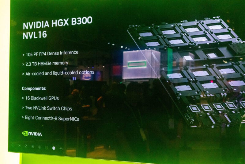
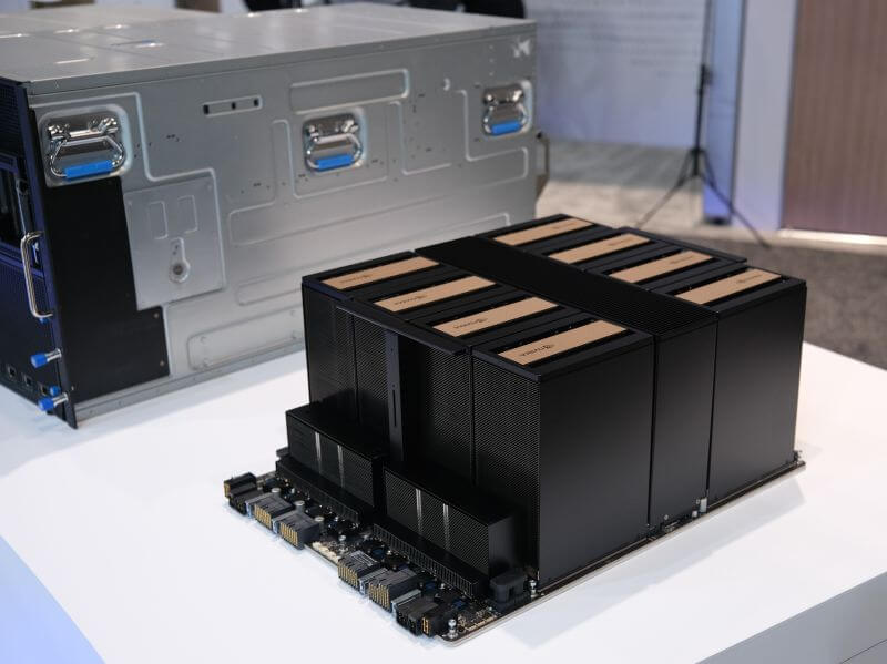
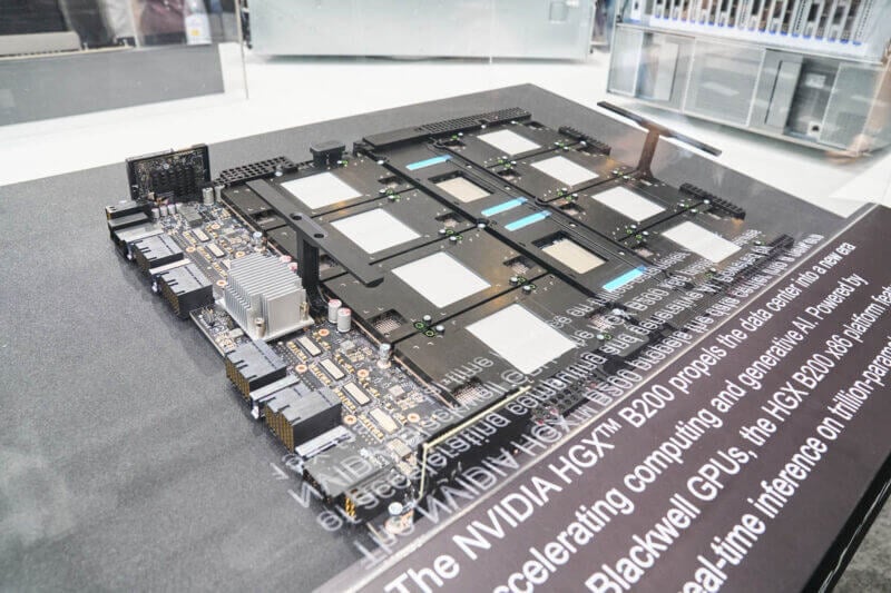
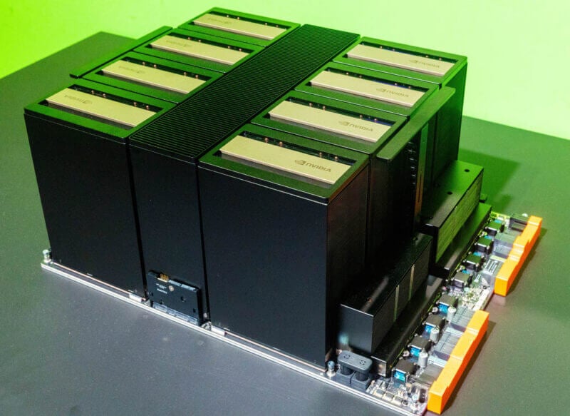
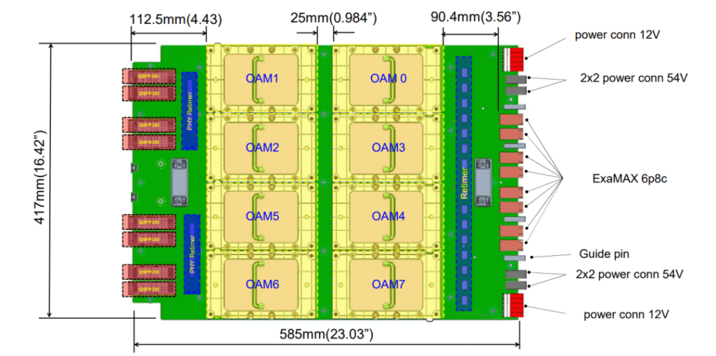
Before the HGX B200, things remained largely the same. However, with the arrival of the NVIDIA HGX B300 NVL16, the landscape is shifting. This platform offers up to 2.3 TB of HBM3e memory. As shown in the image above, it features 16 dual-Blackwell GPU package modules. Last year, NVIDIA upgraded the NVLink switch chips with the HGX B200 design, where two NVLink switch chips are positioned between eight GPU packages. This configuration is similar to what is displayed for the HGX B300 and its components.
In the image below, you can see that the UBB motherboard is equipped with eight large air-cooled heatsinks—each cooling two Blackwell GPUs—with the NVLink switch section situated between them. The module’s height is approximately 5U, as indicated by ASUS’s later-displayed HGX B300 module.
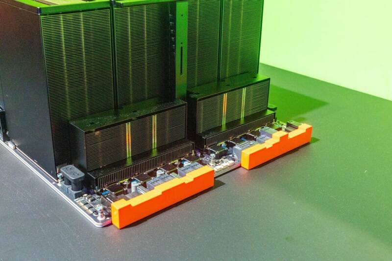
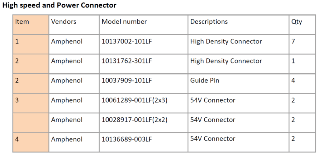
At the end of the UBB, notice an OCP UBB-style connector covered by an orange cap. The high-density connectors (ExaMax connectors) used in the OCP UBB specification by AMD, NVIDIA, and other manufacturers are very fragile, so covering them when they’re not in use is essential.
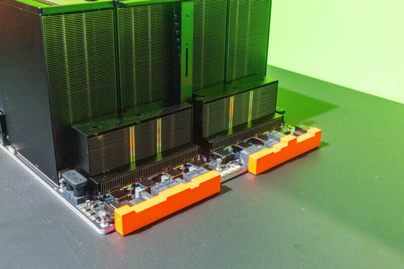
Between these orange-covered connectors and the GPU heatsinks, you can observe smaller heatsinks. These are no longer dedicated to PCIe retimer chips; instead, they now serve NVIDIA ConnectX-8 network interface cards (NICs).
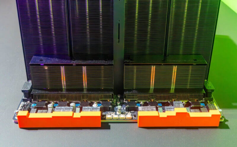
The UBB 2.0 high-speed and power connectors link to the HIB (High-Performance Computing Interface Board). The NIC connectors reside between the UBB connectors and the eight NVIDIA ConnectX-8 NICs mounted on the UBB. A similar view of the HGX H200 shows that those eight upward-facing connectors are absent.
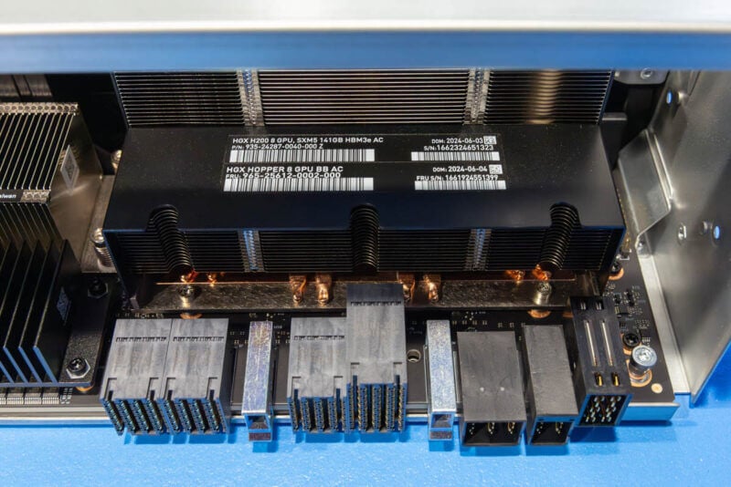
NVIDIA leverages the built-in PCIe switch of the ConnectX-8 to offer features that previously required additional chips. Although this might appear minor, it represents a significant industry shift. At the 2025 NVIDIA GTC conference, ASUS presented the ASUS AI Pod NVIDIA GB300 NVL72 and the ASUS XA NB3I-E12 (a 10U-high module), where the detachable UBB tray at the bottom of the system clearly shows eight network connectivity ports.
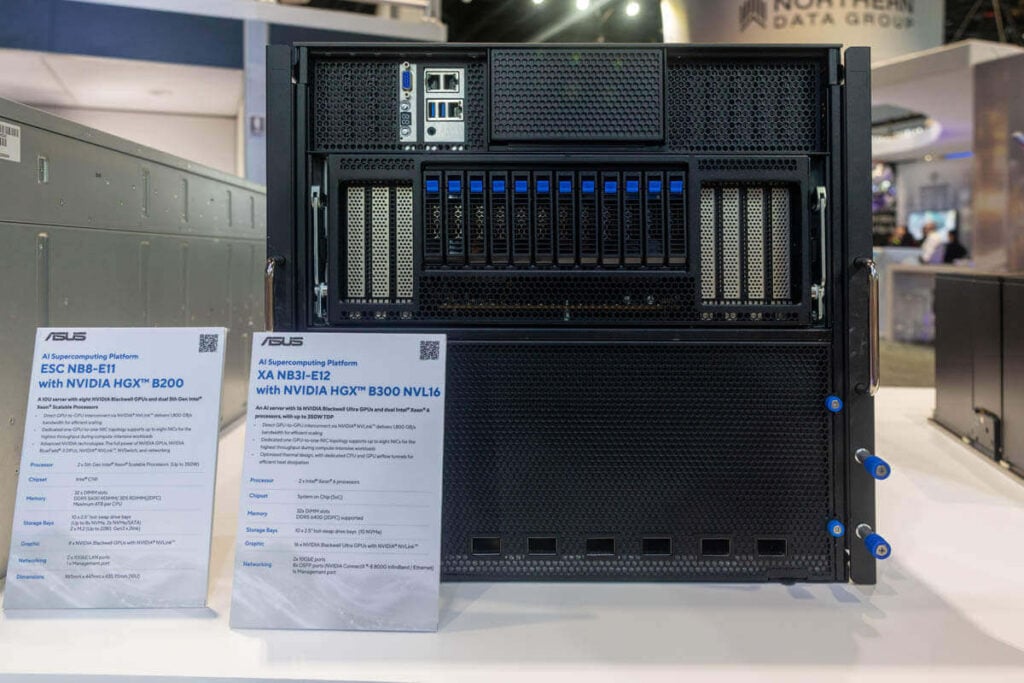
The UBB 1.X motherboard specifications and interface connectors are also highlighted, with the ASUS XA NB3I-E12 being equipped with the NVIDIA HGX B300 NVL16.
Different vendors have designed their trays in various ways. Typically, the interfaces that connect to the external chassis front panel are located on the side opposite the ConnectX-8 NICs, necessitating cabling to bridge this gap. Other vendors are exploring solutions to address this change.