
CPO, or Co-Packaged Optics, is a term often mentioned alongside LPO. Let’s delve into its meaning and significance.
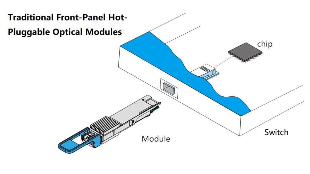
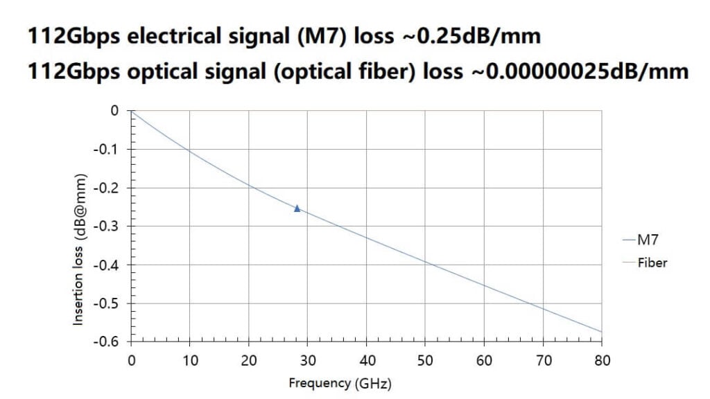
Traditional hot-swappable optical modules connect to the switch system’s main chip via electrical signals over a relatively long distance of approximately 150–200 mm. For instance, in 800G optical modules utilizing M7 PCB interconnects, signal loss for 112Gbps PAM4 signals (with ~30 GHz bandwidth) is approximately 0.25 dB/mm. By comparison, the loss in optical fibers for such signals is millions of times smaller, rendering it negligible. Furthermore, electrical signal loss increases with frequency, whereas optical signal loss remains constant regardless of frequency. This constancy is attributed to optical signals being modulated onto an optical carrier wave, which has a fixed frequency (e.g., 228THz for a 112Gbps PAM4 signal).
Two primary strategies exist to reduce electrical signal loss:
- Using low-loss conductive and dielectric materials.
- Reducing interconnect distances.
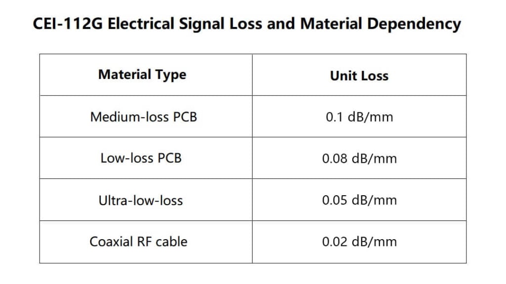
CPO adopts the second approach. It integrates the CPO optical module with the ASIC (Application-Specific Integrated Circuit) chip in the switch, thereby shortening interconnect distances and reducing high-frequency RF signal loss.
Signal Standards and Industry Definitions
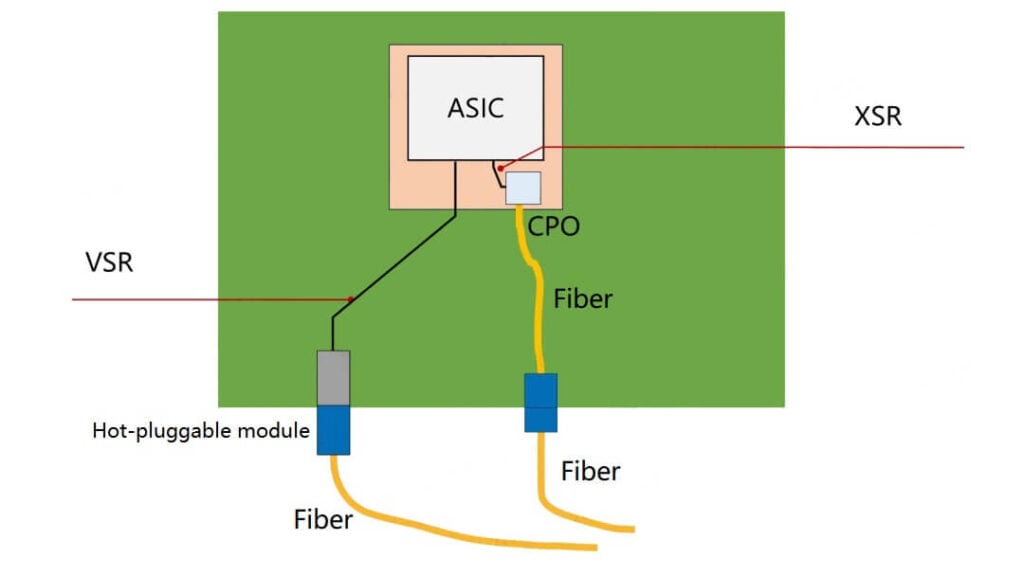
- VSR: Defined by the CEI standard for electrical signals between front-panel optical modules and ASIC chips.
- XSR: Defined by the CEI standard for electrical signals between co-packaged CPO modules and ASIC chips.
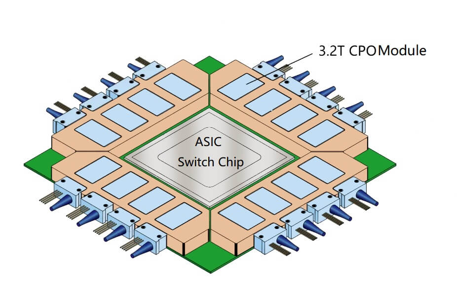
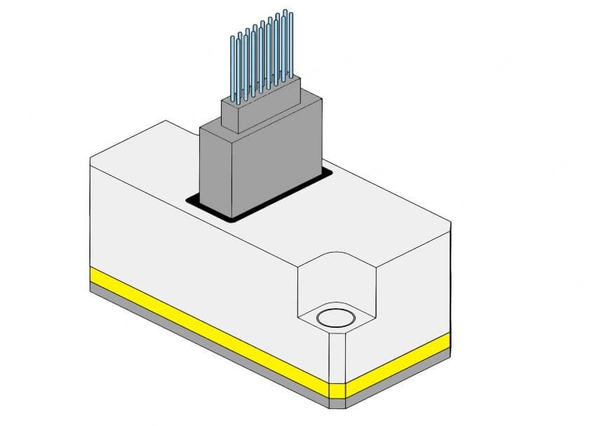
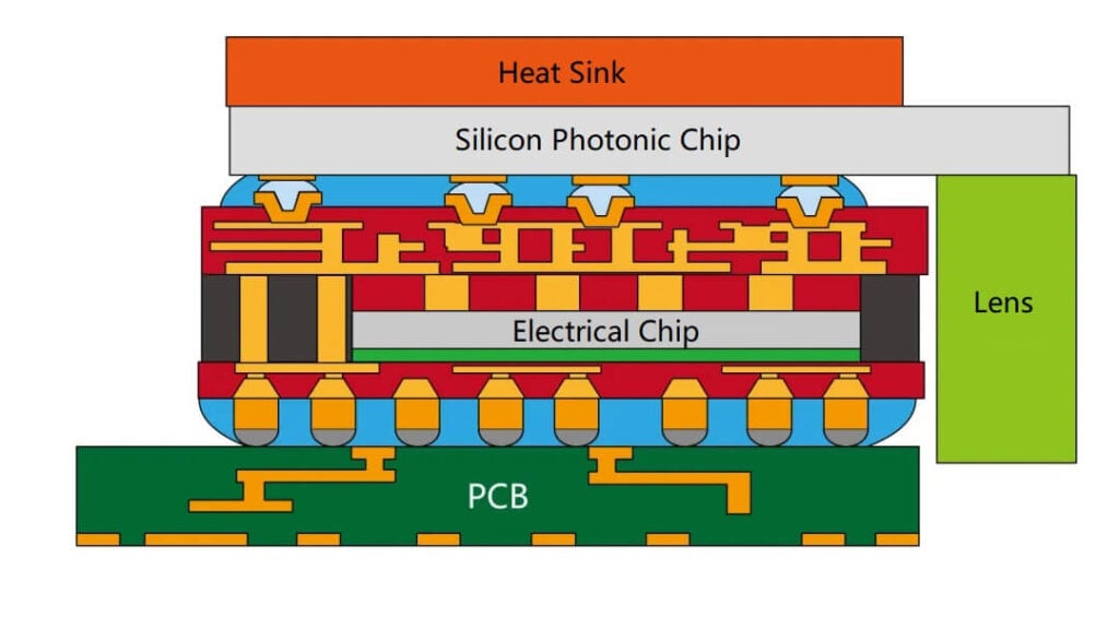
In OIF standards, the 3.2Tbps CPO module is defined. The picture below represents an integration of a 51.2Tbps switch with a 3.2Tbps CPO module. CPO refers to the “co-packaging” with the ASIC chip to minimize electrical signal distances and address significant insertion loss challenges at high frequencies.
The OIF CPO standard specifies single-mode communication and compact module designs. This effectively excludes VCSEL technology, favoring silicon photonics for its ability to accommodate tight layouts.
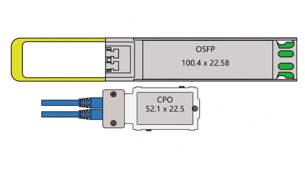
OSFP modules, currently common for 800Gbps optical modules, are distinct from the CPO standard, which defines a capacity of 8x400Gbps (3.2Tbps per module). This requires far greater capacity within limited layouts, necessitating deep integration with silicon photonics due to challenges with EML or InP integration.
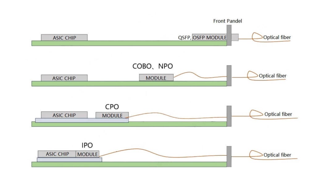
CPO’s Evolution and Related Concepts Introduced around 2018, the CPO concept has absorbed earlier non-hot-swappable optical technologies like OBO, OBA, and COBO (2010–2018), which are now collectively referred to as CPO. Further, based on the proximity of integration with the ASIC, there are subcategories:
NPO (Near-Packaged Optics): For relatively distant integrations.
IPO (In-Package Optics): For closer integrations.
CPO remains a groundbreaking approach to addressing challenges in high-frequency signal loss and scaling optical communication capacities in modern systems.
Broadly speaking, if all non-hot-pluggable optical modules are categorized as CPO (Co-Packaged Optics), then the term is no longer limited to single-mode communication as currently defined by standards. Consequently, certain multi-mode CPO concepts have emerged in the industry.
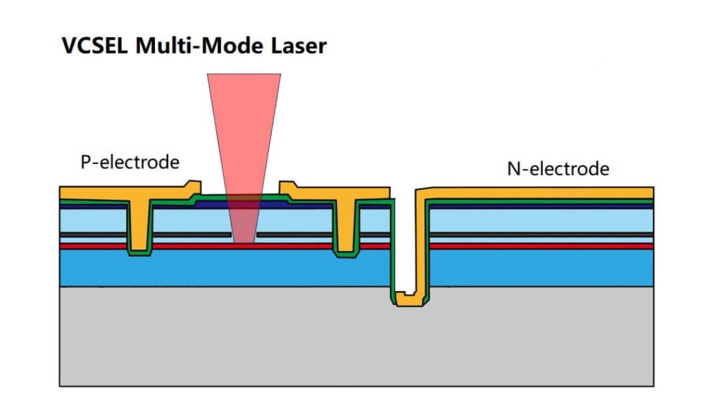
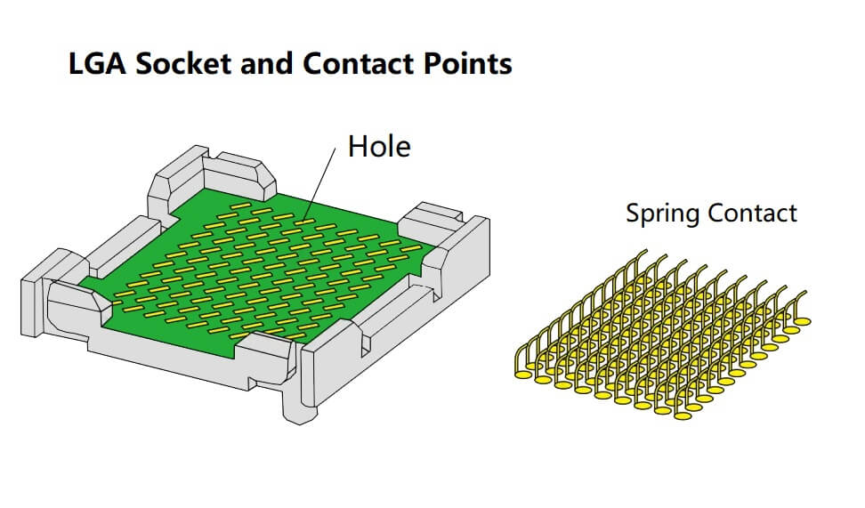
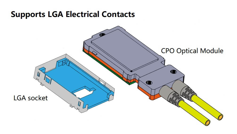
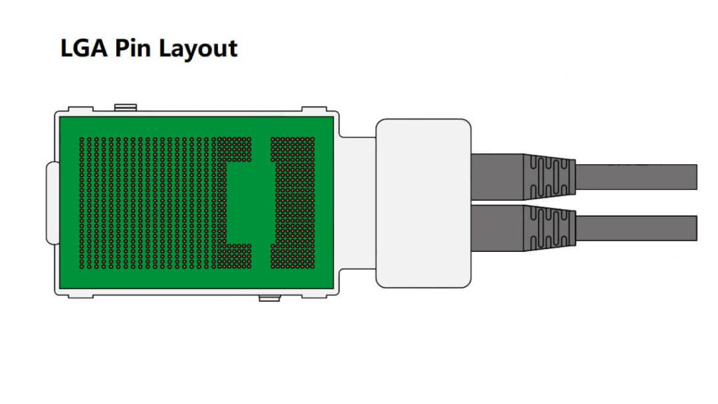
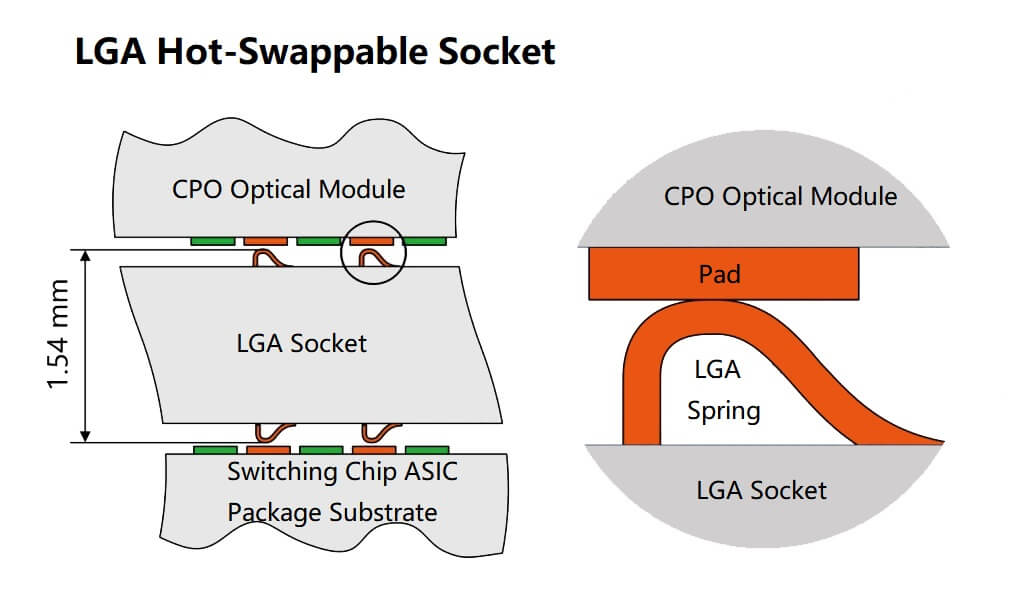
Multi-mode CPO systems utilize multi-mode VCSELs (Vertical Cavity Surface Emitting Lasers) paired with photodetectors (PDs). For example, Japanese manufacturers like Fujitsu and Furukawa have introduced 400Gbps multi-mode CPO optical modules using LGA (Land Grid Array) press-fit contact grids.
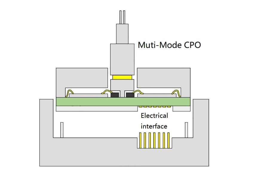
Similarly, American companies such as Finisar (now Coherent) and HP have adopted multi-mode CPO solutions with capacities ranging from 1-2Tbps, supporting VCSEL arrays like 16-channel or 24-channel configurations. These systems also utilize LGA contacts.
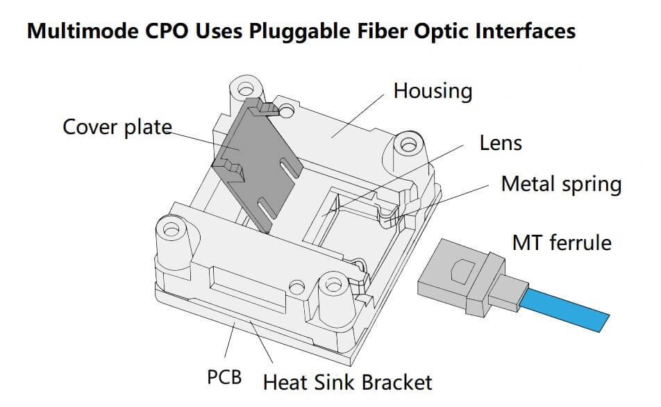
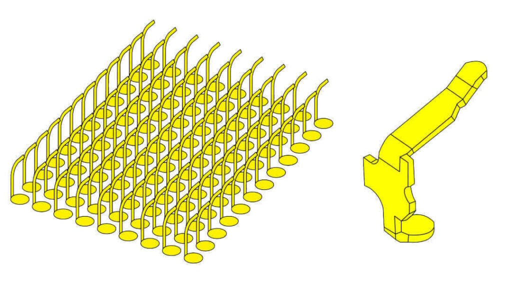
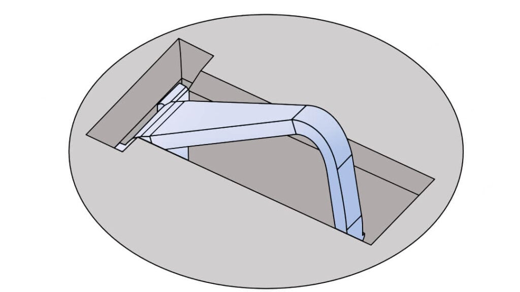
LGA Advantages in Multi-Mode CPO Unlike traditional soldering, LGA connections rely on press-fit contacts, eliminating the need for reflow soldering. This facilitates easier CPO assembly and maintenance while avoiding material stress due to mismatched thermal expansion coefficients (CTEs) during high-temperature soldering. Additionally, it prevents issues caused by glue curing under heat, which could otherwise affect optical alignment.
Differences Between Silicon Photonics CPO and Multi-Mode VCSEL CPO Narrowly defined CPO solutions based on silicon photonics differ significantly from broader multi-mode VCSEL-based CPO systems:
Power Consumption: Single-mode silicon photonic CPO systems consume more power than multi-mode VCSEL-based systems.
Reliability: Silicon photonic systems exhibit higher reliability, as silicon (an elemental semiconductor) presents lower failure risks compared to compound semiconductors used in VCSEL systems, which are more prone to reliability challenges.
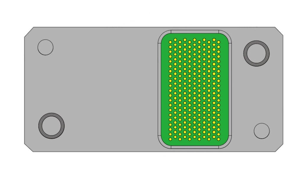
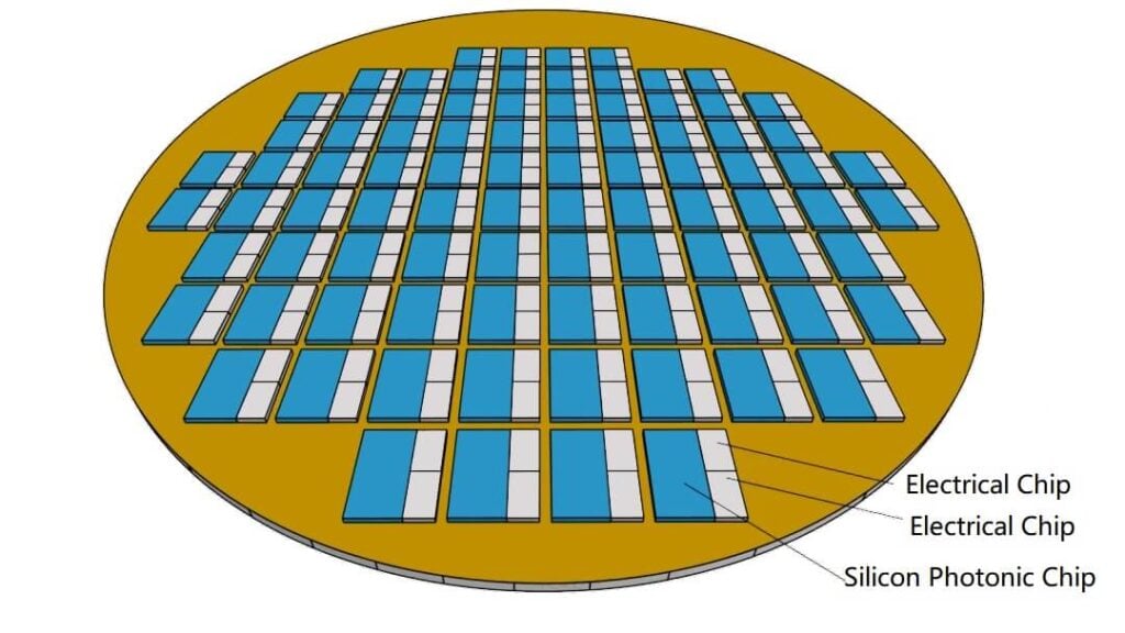
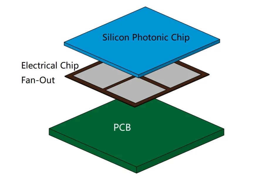
Single-Mode CPO and Integration Challenges Returning to single-mode CPO as defined by OIF, using silicon photonic integrated chips complicates packaging processes compared to traditional hot-pluggable optical modules. For instance, space is extremely constrained with ASIC chips measuring ~30mm and CPO widths of ~20mm. Each CPO includes 32 Tx differential pairs, 32 Rx differential pairs, and control signal lines, necessitating ultra-high-density layouts for electrical signals.
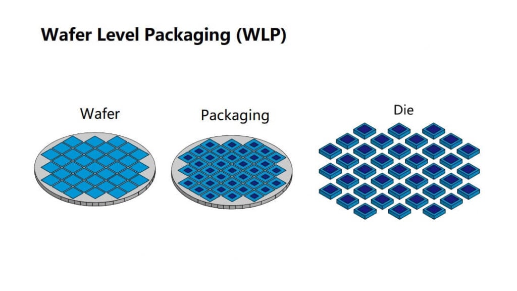
Conventional wire bonding cannot meet these density demands, prompting most manufacturers to adopt advanced technologies like TCB (Thermo-Compression Bonding) or wafer-level packaging, such as Intel’s approach, or at minimum, flip-chip methods.
Wafer-level packaging is particularly under intense research for 2024-2025 commercialization. It leverages semiconductor processes to achieve finer lines, smaller vias, and denser interconnects. After achieving high-density connections, wafers are diced into dies and assembled into CPOs.
Advanced Through-Via Technologies for High-Density Interconnects Wafer-level assembly may utilize different via technologies, depending on interconnect requirements:
TSV (Through-Silicon Vias): Supporting up to ~30GHz bandwidth (~112Gbps PAM4 signals), but with significant parasitic capacitance due to silicon’s semiconductor properties. This can lead to resonances.
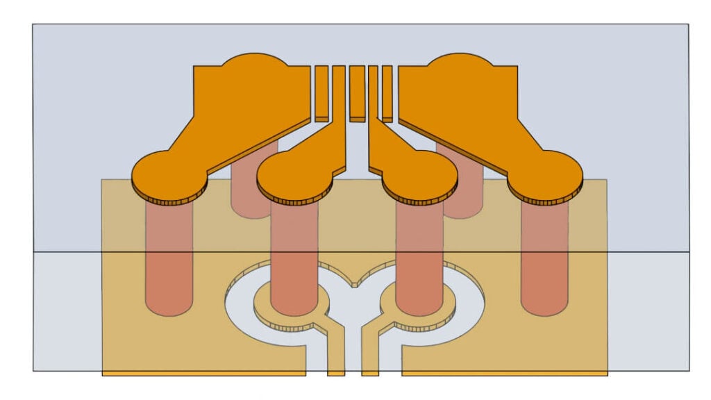
TGV (Through-Glass Vias): Offers better bandwidth but is fragile due to glass’s rigidity.
TMV (Through-Molded Vias): Features a molded structure using RF dielectric materials to fill via gaps, supporting larger bandwidths while addressing challenges like thermal expansion.
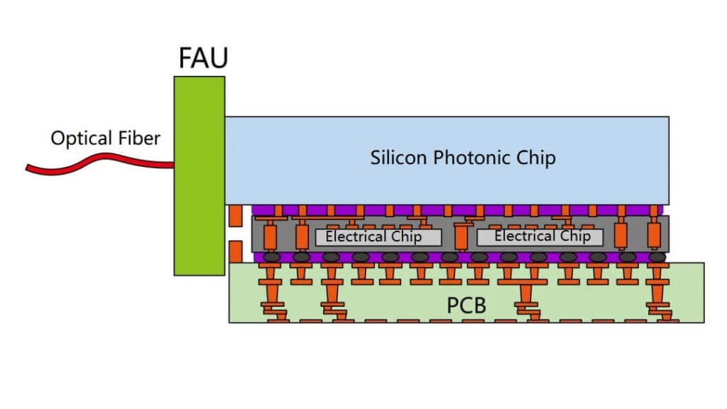
Optical Packaging Challenges in CPO Apart from electrical interconnect densities, CPO optical packaging is also more demanding than traditional optical modules. For example, a 3.2Tbps CPO includes 32x112Gbps channels for both Tx and Rx, requiring 64 optical fibers in a non-WDM setup. WDM (e.g., 4-wavelength WDM) reduces this to 16 fibers.
Optical fiber alignment poses two challenges:
The optical fiber mode field diameter is larger than the waveguide mode field of silicon photonics, necessitating mode field converters (e.g., spot-size converters or SSCs).
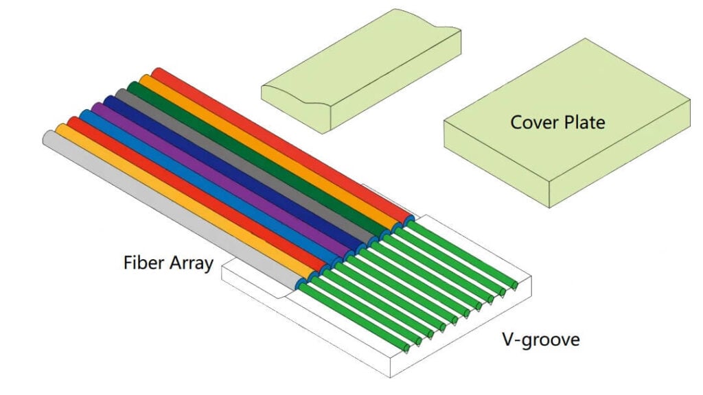
Various designs, such as inverted taper structures, trident shapes, or diamond-like configurations, aim to expand the optical field while optimizing production costs and consistency.
Laser Integration Approaches
Finally, laser selection is critical in silicon photonics-based CPO systems.
Options include:
Integrated Lasers: Higher integration but higher failure rates (e.g., Intel).
Flip-Chip Lasers: Moderate integration and reliability (e.g., Marvell).
External Laser Sources (ELSFP): Independent laser modules providing CW light for CPOs, offering higher reliability at the cost of increased optical loss.
CPO also requires managing stress in optical fibers, as these glass materials are susceptible to stress under bending or compression. Solutions involve optimized fiber design and assembly processes, such as low-temperature adhesive techniques or advanced soldering methods (e.g., laser welding, glass welding).
This comprehensive framework highlights both the innovations and technical hurdles shaping the evolution of CPO systems.
Related Products:
-
 OSFP-800G-FR4 800G OSFP FR4 (200G per line) PAM4 CWDM Duplex LC 2km SMF Optical Transceiver Module
$5000.00
OSFP-800G-FR4 800G OSFP FR4 (200G per line) PAM4 CWDM Duplex LC 2km SMF Optical Transceiver Module
$5000.00
-
 OSFP-800G-2FR2L 800G OSFP 2FR2 (200G per line) PAM4 1291/1311nm 2km DOM Duplex LC SMF Optical Transceiver Module
$4500.00
OSFP-800G-2FR2L 800G OSFP 2FR2 (200G per line) PAM4 1291/1311nm 2km DOM Duplex LC SMF Optical Transceiver Module
$4500.00
-
 OSFP-800G-2FR2 800G OSFP 2FR2 (200G per line) PAM4 1291/1311nm 2km DOM Dual CS SMF Optical Transceiver Module
$4500.00
OSFP-800G-2FR2 800G OSFP 2FR2 (200G per line) PAM4 1291/1311nm 2km DOM Dual CS SMF Optical Transceiver Module
$4500.00
-
 OSFP-800G-DR4 800G OSFP DR4 (200G per line) PAM4 1311nm MPO-12 500m SMF DDM Optical Transceiver Module
$3500.00
OSFP-800G-DR4 800G OSFP DR4 (200G per line) PAM4 1311nm MPO-12 500m SMF DDM Optical Transceiver Module
$3500.00
-
 NVIDIA MMS4X00-NM-FLT Compatible 800G Twin-port OSFP 2x400G Flat Top PAM4 1310nm 500m DOM Dual MTP/MPO-12 SMF Optical Transceiver Module
$900.00
NVIDIA MMS4X00-NM-FLT Compatible 800G Twin-port OSFP 2x400G Flat Top PAM4 1310nm 500m DOM Dual MTP/MPO-12 SMF Optical Transceiver Module
$900.00
-
 NVIDIA MMA4Z00-NS-FLT Compatible 800Gb/s Twin-port OSFP 2x400G SR8 PAM4 850nm 100m DOM Dual MPO-12 MMF Optical Transceiver Module
$650.00
NVIDIA MMA4Z00-NS-FLT Compatible 800Gb/s Twin-port OSFP 2x400G SR8 PAM4 850nm 100m DOM Dual MPO-12 MMF Optical Transceiver Module
$650.00
-
 NVIDIA MMS4X00-NM Compatible 800Gb/s Twin-port OSFP 2x400G PAM4 1310nm 500m DOM Dual MTP/MPO-12 SMF Optical Transceiver Module
$900.00
NVIDIA MMS4X00-NM Compatible 800Gb/s Twin-port OSFP 2x400G PAM4 1310nm 500m DOM Dual MTP/MPO-12 SMF Optical Transceiver Module
$900.00
-
 NVIDIA MMA4Z00-NS Compatible 800Gb/s Twin-port OSFP 2x400G SR8 PAM4 850nm 100m DOM Dual MPO-12 MMF Optical Transceiver Module
$650.00
NVIDIA MMA4Z00-NS Compatible 800Gb/s Twin-port OSFP 2x400G SR8 PAM4 850nm 100m DOM Dual MPO-12 MMF Optical Transceiver Module
$650.00
-
 NVIDIA MMS1Z00-NS400 Compatible 400G NDR QSFP112 DR4 PAM4 1310nm 500m MPO-12 with FEC Optical Transceiver Module
$700.00
NVIDIA MMS1Z00-NS400 Compatible 400G NDR QSFP112 DR4 PAM4 1310nm 500m MPO-12 with FEC Optical Transceiver Module
$700.00
-
 NVIDIA MMS4X00-NS400 Compatible 400G OSFP DR4 Flat Top PAM4 1310nm MTP/MPO-12 500m SMF FEC Optical Transceiver Module
$700.00
NVIDIA MMS4X00-NS400 Compatible 400G OSFP DR4 Flat Top PAM4 1310nm MTP/MPO-12 500m SMF FEC Optical Transceiver Module
$700.00
-
 NVIDIA MMA1Z00-NS400 Compatible 400G QSFP112 SR4 PAM4 850nm 100m MTP/MPO-12 OM3 FEC Optical Transceiver Module
$550.00
NVIDIA MMA1Z00-NS400 Compatible 400G QSFP112 SR4 PAM4 850nm 100m MTP/MPO-12 OM3 FEC Optical Transceiver Module
$550.00
-
 NVIDIA MMA4Z00-NS400 Compatible 400G OSFP SR4 Flat Top PAM4 850nm 30m on OM3/50m on OM4 MTP/MPO-12 Multimode FEC Optical Transceiver Module
$550.00
NVIDIA MMA4Z00-NS400 Compatible 400G OSFP SR4 Flat Top PAM4 850nm 30m on OM3/50m on OM4 MTP/MPO-12 Multimode FEC Optical Transceiver Module
$550.00
-
 NVIDIA MMS4X50-NM Compatible OSFP 2x400G FR4 PAM4 1310nm 2km DOM Dual Duplex LC SMF Optical Transceiver Module
$1200.00
NVIDIA MMS4X50-NM Compatible OSFP 2x400G FR4 PAM4 1310nm 2km DOM Dual Duplex LC SMF Optical Transceiver Module
$1200.00
-
 OSFP-XD-1.6T-4FR2 1.6T OSFP-XD 4xFR2 PAM4 1291/1311nm 2km SN SMF Optical Transceiver Module
$17000.00
OSFP-XD-1.6T-4FR2 1.6T OSFP-XD 4xFR2 PAM4 1291/1311nm 2km SN SMF Optical Transceiver Module
$17000.00
-
 OSFP-XD-1.6T-2FR4 1.6T OSFP-XD 2xFR4 PAM4 2x CWDM4 2km Dual Duplex LC SMF Optical Transceiver Module
$22400.00
OSFP-XD-1.6T-2FR4 1.6T OSFP-XD 2xFR4 PAM4 2x CWDM4 2km Dual Duplex LC SMF Optical Transceiver Module
$22400.00
-
 OSFP-XD-1.6T-DR8 1.6T OSFP-XD DR8 PAM4 1311nm 2km MPO-16 SMF Optical Transceiver Module
$12600.00
OSFP-XD-1.6T-DR8 1.6T OSFP-XD DR8 PAM4 1311nm 2km MPO-16 SMF Optical Transceiver Module
$12600.00