
In recent years, AI server clusters have grown significantly in size. Optical links, due to their scalability and cost advantages, provide the necessary connections for long-distance expansion of these clusters. Broadcom is a leader in the three core optical interconnect technologies essential for building large-scale AI networks.
Vertical-Cavity Surface-Emitting Laser (VCSEL)
VCSEL is the mainstay of optical AI interconnect technology across the industry. Its low power consumption and cost make it an ideal choice for data communication and sensing applications. The only limitation is its operation over shorter connection distances. The 4x100G VCSEL has already been mass-produced, and the 4x200G version is expected to be sampled in the second half of 2024.
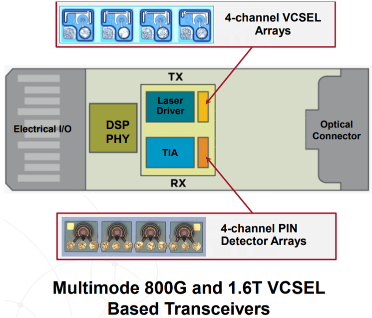
Broadcom’s VCSEL technology has consistently led the industry in terms of time-to-market, volume, performance, and reliability. At OFC2024, Broadcom achieved the latest advancements in 200G/lane VCSEL, demonstrating transmission over 100m OM3 fiber at 100 GBd PAM4 and 53.125 GBd PAM4, maintaining its leadership position.
Electro-Absorption Modulated Laser (EML)
EML is ideal for extending AI systems to greater distances, scaling to hundreds of thousands or even millions of units. This technology offers better performance at very high bandwidths, with the next-generation data rates set for mass deployment. Notably, Broadcom has expanded EML technology from 100G/lane to 200G/lane and achieved large-scale production.
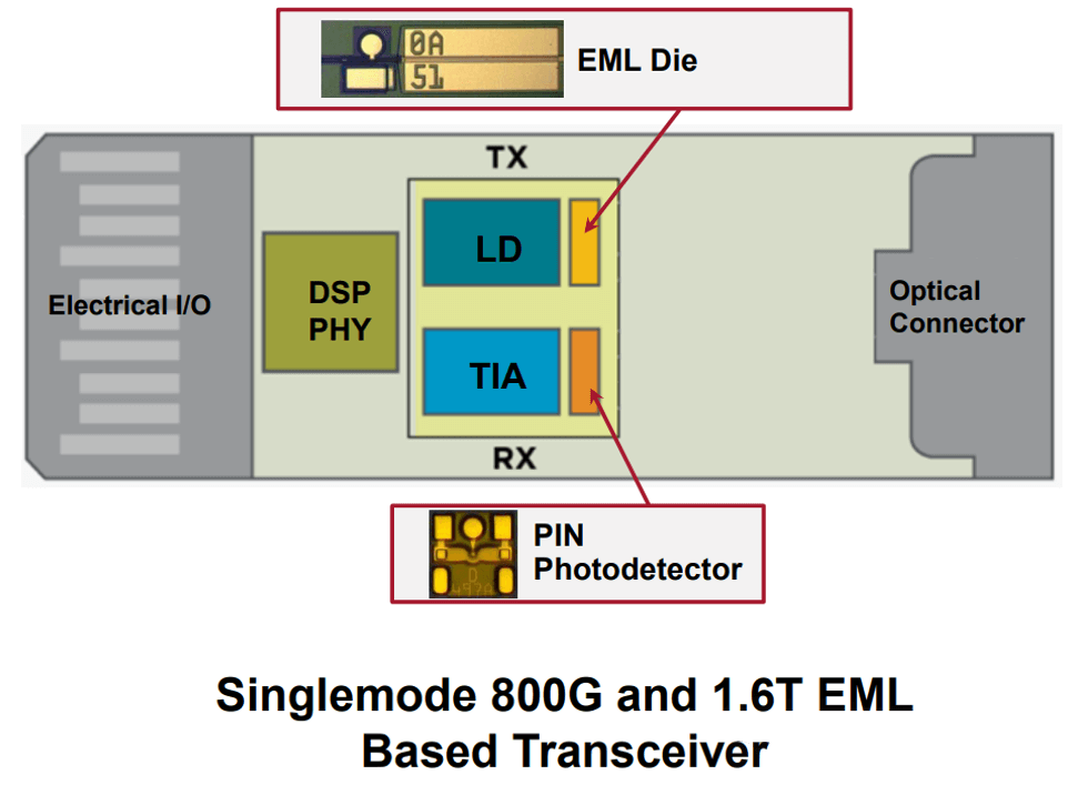
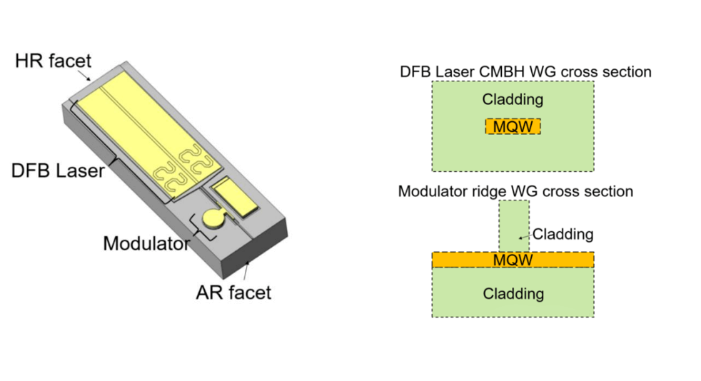
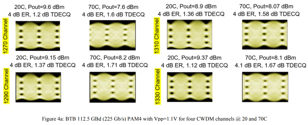
At OFC2023, Broadcom reported a four-channel O-band CWDM system based on a CMBH EML, applicable to 800G DR4/FR4 and 1.6T. This EML operates at 20-70°C, with a lumped electrode 3dB EO-BW exceeding 60 GHz, suitable for 200G/lane applications. The 112.5 GBd BTB PAM4 ER is 4 dB, with an output power greater than 7 dBm. The TDECQ for 100Gbd transmission over 2 kilometers is less than 3.25 dB.
Co-Packaged Optics (CPO)
CPO integrates advanced high-speed silicon photonics heterogeneously into specific integrated circuits to address next-generation bandwidth and power challenges. This new technology provides power and cost advantages for future generations of AI systems and enables infrastructure to support large-scale AI networks.
At OFC2024, Broadcom showcased its 51.2T Bailly CPO (Co-Packaged Optics), marking the first commercial shipment. The complete optical link is directly integrated into the package, with all 512 channels optically connected to the switch itself.
It uses eight FR4 silicon photonics engines, each with 64 channels of 6.4T, totaling 51.2T. The laser light source is externally pluggable.
Broadcom identifies several core advantages of adopting Co-Packaged Optics (CPO) technology:
Cost Reduction: As bandwidth and the number of components increase, silicon photonics technology allows for more components to be placed on a single chip, thereby reducing costs.
Power Efficiency: This layout eliminates the complex electronic channels between ASICs and optical devices, significantly reducing power consumption. A typical 800G pluggable transceiver consumes about 16W per link, whereas a CPO system reduces the optical link power to 5W. For 1.6T, conventional pluggable transceivers consume 25W, while CPO consumes only 8W.
Enhanced Reliability: Pluggable transceivers have a failure rate of approximately 2%. By integrating more components into the chip, CPO enhances reliability. Broadcom’s approach involves making the laser a pluggable and easily replaceable component within the system, with everything else built on core silicon technology.
Broadcom offers a range of high-power single-mode DFB laser diode chips, with wavelengths spanning the O to C bands, serving as external light sources for silicon photonics. These chips, based on CMBH structures, provide output power ranging from 20 to 100mW and support non-cooled applications.
As AI and machine learning systems continue to accelerate, Meta Platforms, Inc. highlighted at the 2022 OCP Global Summit the growing gap between computing power and interconnect bandwidth. To bridge this gap, architectural and design paradigms need to shift from packet-based to network-based approaches.
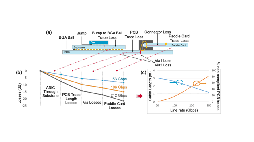
In hyperscale networks, switches are typically configured in spine and leaf arrangements. Almost all spine-leaf connections are optical, using active optical cables (AOCs), multimode (MM), single-mode (SM), or coherent transceivers to achieve distances beyond 3 meters. Within racks, nearly everything is connected via direct attach copper (DAC) cables, limited to distances under 3 meters. Regardless of whether switches are in the spine or leaf, all switches use in-box copper to connect the core ASIC to the front panel.
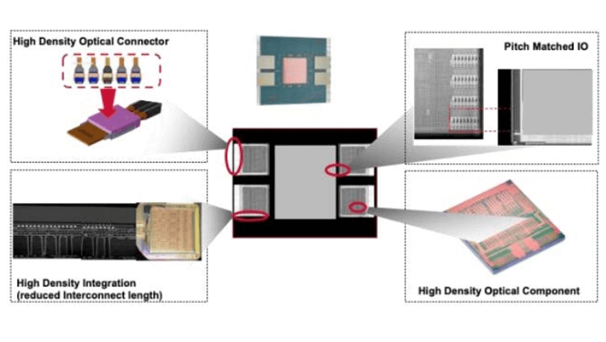
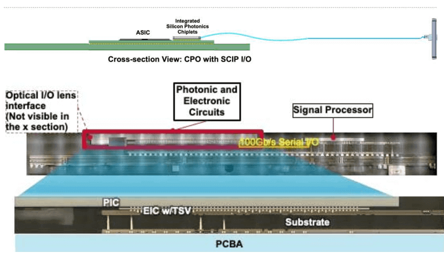
As illustrated below, when signals pass through the core silicon, they experience various transitions (e.g., bumps, vias, ball grid arrays (BGAs), electrical connectors) and path lengths (PCB traces, substrate routing, card traces), leading to distortion. When channel data rates exceed 200Gbps, these distortions become challenging for timing, resulting in increased bit error rates or uncorrectable errors. For switches deploying optical solutions, the power required for connections increases, straining thermal cooling and power delivery systems. The optimal solution for low-cost, high-performance, low-power, and reliability requirements is in the form of Silicon Chip Integrated Photonics (SCIP).
SCIP shortens the high-speed routing distance between the ASIC and silicon photonics chip, achieving extremely low insertion loss and thereby improving energy efficiency to less than 1pJ/bit. SCIP employs TSV technology to achieve the shortest interconnect length between PIC (Photonic Integrated Circuit) and EIC (Electrical Integrated Circuit) chips.
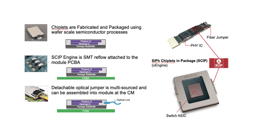
Broadcom believes that the SCIP (Silicon Chip Integrated Photonics) solution should adhere to two key principles:
- Compatibility with Manufacturing and Packaging Processes: The solution should be compatible with silicon chips (maintaining IO pitch matching) and packaging (providing solder reflow packaging). By utilizing the latest semiconductor processes, such as those used for high-bandwidth memory (HBM), lasers can be remotely placed on the optical engine, freeing up space in very limited areas and significantly reducing the overall system power consumption.
- Detachable Optical Interconnect with oEngine: The optical connector must not only maintain high density as per the first principle but also be detachable. Due to the higher failure rate of lasers, higher drive currents are needed to overcome thermal environments, necessitating some redundancy in the lasers. The SCIP platform, with 3D chip stacking and detachable optical connectors, can be co-packaged with digital signal processors (DSPs) or switch ASICs in transceiver form, flexibly scaling from 400Gbps FR4 or DR4 to 3.2Tbps DR or 6.4Tbps FR4.
With these principles established, we can now focus on optical IO.
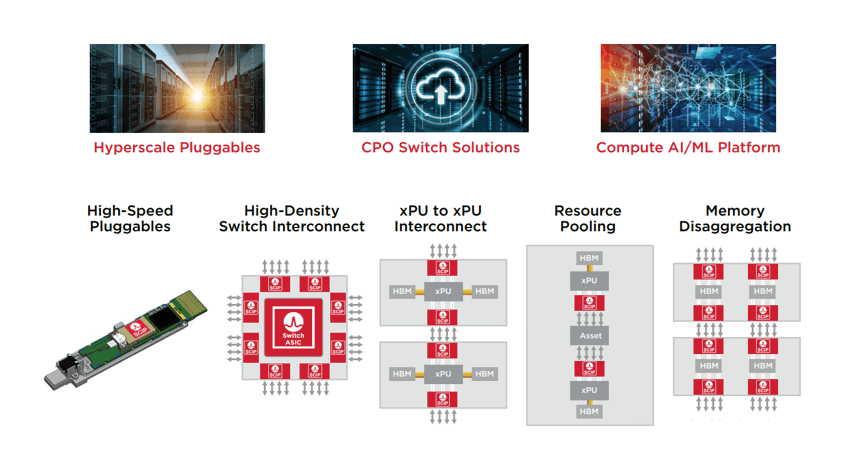
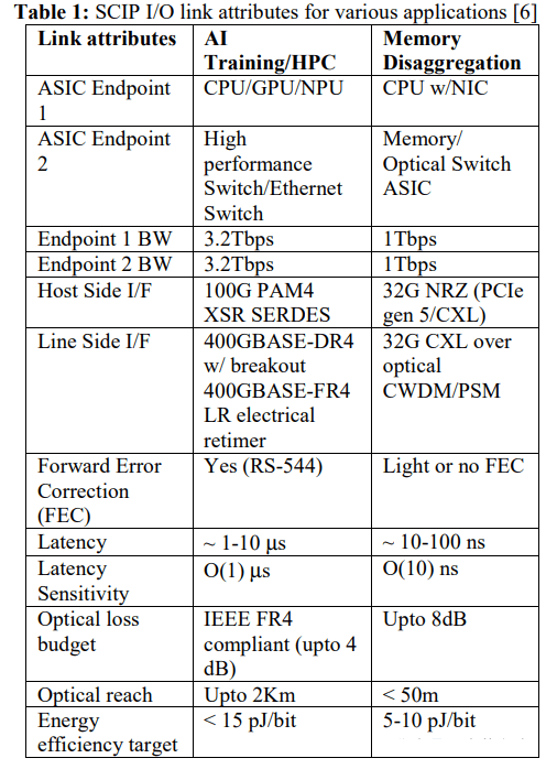
The CPO (Co-Packaged Optics) link based on SCIP I/O can be used for various connections within data centers, including traditional data center network layers, AI training/high-performance computing links, resource pooling, and memory disaggregation, as shown below. The first application is that the PCIe link based on SCIP I/O can provide scalable solutions for various clusters (NPU, GPU, CPU, memory, storage, and network interface cards (NICs)). The second application is that the CXL link through SCIP I/O can be used for memory disaggregation, where multiple CPUs are interconnected with multiple memory units via an optical switch.
Broadcom’s SCIP I/O chip stacking is assembled using CoW (Chip-on-Wafer) technology, with the cross-section as follows: The EIC (Electrical Integrated Circuit) is connected to a glass carrier after foundry processing for backside thinning, followed by TSV (Through-Silicon Via) DRIE (Deep Reactive Ion Etching) processing, with a TSV pitch of 130um. A single RDL (Redistribution Layer) plating is used to fill the TSV and form routing wires. Then, CuP (Copper Pillar) interconnects are formed on the backside of the EIC to fill and thermocompression bond to the PIC (Photonic Integrated Circuit) chip. The wafer is then stealth diced. Finally, the ASIC and SCIP are co-packaged, with the ASIC bonded to the substrate using SMT (Surface-Mount Technology) and the SCIP bonded to the substrate using a no-flux reflow process, ensuring no water wash or flux residue contaminates the optical components.
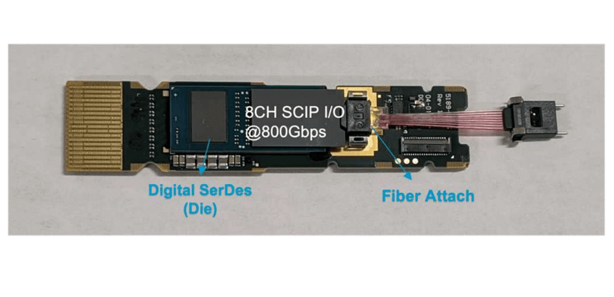
Broadcom’s SCIP I/O demonstration comes in two forms:
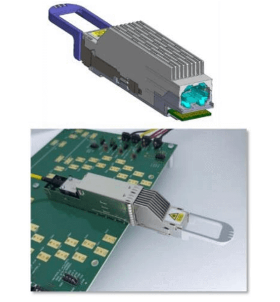
- 8-channel SCIP I/O: This is packaged with an ASIC, providing a total bandwidth of 800Gb/s, suitable for MSA-defined QSFP-DD transceivers. The SCIP integrates lasers and a detachable optical connector interface.
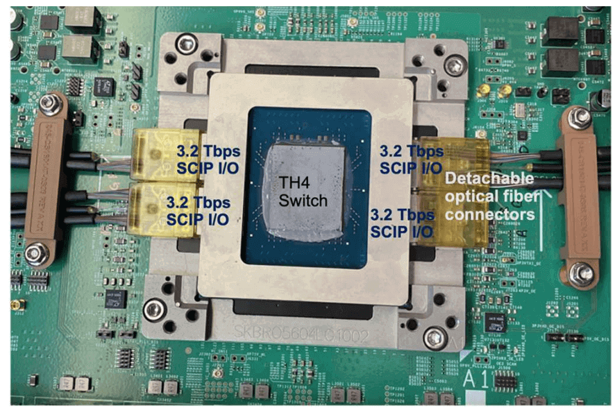
- 4 x 32CH SCIP I/O: This is packaged with a 25.6Tb/s Ethernet switch. The CPO has an optical I/O bandwidth of 12.8Tb/s, with the other half used for high-speed electrical I/O transmission. Each SCIP has a detachable optical fiber connector for optical interfaces. The system supports remote laser configuration, where optical power is supplied to the SCIP through the optical connector interface.
The remote laser source module follows the pluggable QSFP DD package. Each channel’s optical power specification can reach up to 21 dBm, with good repeatability.
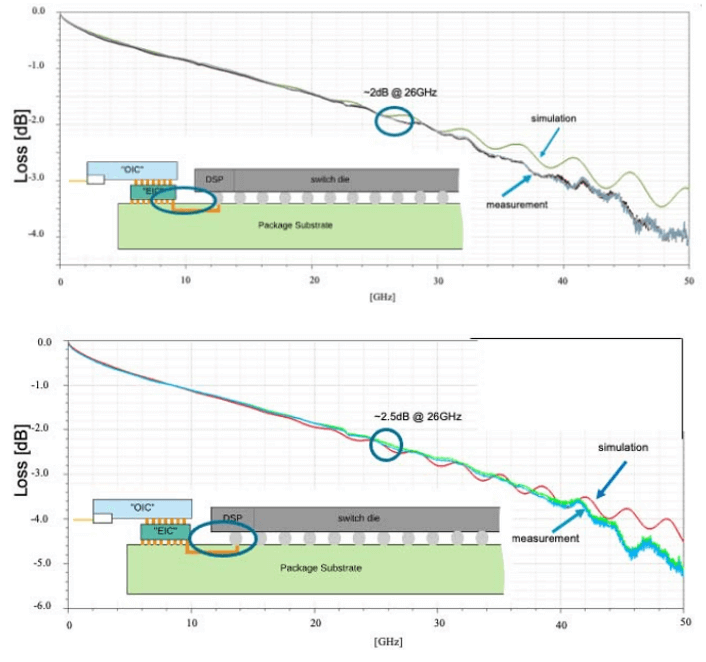
The diagram below shows the electrical channel loss for the transmission and reception paths between the optical engine and the switch ASIC. Standard architectures require electrical insertion loss up to 20dB, but the co-packaged system’s equivalent insertion loss is only 2-3dB. The interface has very low power consumption, with traditional optical transceiver modules consuming 15-20pJ/bit, while the co-packaged technology consumes only 5-10pJ/bit, reducing the power required for the optical interface by half.
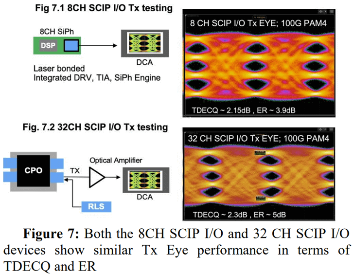
The transmission performance of the SCIP I/O link is measured at the host interface under 100G/lane PAM4 modulation. The 8-channel SCIP I/O has a TDECQ of approximately 2.15 – 2.7 dB and an ER of about 3.85 – 4.1 dB. The 32-channel SCIP I/O has a TDECQ of 1.8 – 2.3 dB and an ER of about 4 – 5 dB.
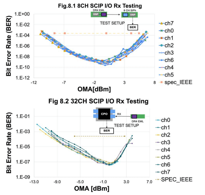
The interconnect receiver performance evaluation is based on pre-FEC bit error rate (BER) measurements. The BER is typically plotted as a function of optical modulation amplitude (OMA) and has a bathtub shape, with the optimal OMA (BER floor) having the lowest BER. Below the optimal OMA, the BER increases due to noise, while above the optimal OMA, the BER increases due to nonlinearity associated with transimpedance amplifier (TIA) overload limitations. The 8-channel SCIP I/O has a BER of approximately 1e-9, and the 32-channel SCIP I/O has a BER of approximately 1e-7. The 32-channel SCIP I/O directly drives the optical interface without any DSP in the path. Thus, SCIP I/O reduces power consumption and cost by eliminating additional DSP in the path while providing comparable performance.
In summary, SCIP-based optical I/O offers two advantages: reducing routing complexity and increasing the physical distance between clusters. The SCIP solution can bridge the gap between the computational capabilities of real systems and those brought by technological nodes, providing more bandwidth for external clusters and improving the overall system’s I/O efficiency.