
Recently, Synopsys announced the industry’s first complete PCIe 7.0 IP solution, including controller, IDE security module, PHY and verification IP. Among them, the verification IP is now available, and the PCIe 7.0 controller (with IDE security function) and PHY IP for advanced processes are planned to be fully available in early 2025. The IP solution improves interconnect power efficiency by up to 50 percent and doubles interconnect bandwidth for the same chip perimeter compared to the previous generation PCIe.
In addition, Synopsys’ PCIe 7.0 PHY IP provides excellent signal integrity, up to 128Gb/s per lane, and seamlessly integrates with Synopsys’ CXL controller IP solution. It also provides excellent signal integrity and data encryption capabilities to effectively prevent hardware attacks while supporting broad ecosystem interoperability. The launch of this program has received strong support from many leading technology companies around the world, including Intel, Astera Labs, Enfabrica, Kandou, Rivos and Microchip.
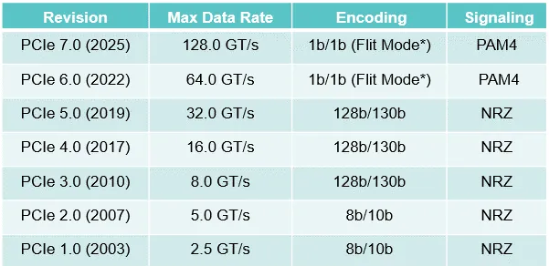
What exactly is updated in PCIe 7.0? First of all, there is no doubt that the data rate has doubled again. The data rate of PCIe 6.0 is 64GT/s, and that of 7.0 is 128GT/s, which is amazing! The speed of a single Lane is 128GT, which is 16GB/s when converted into GB. An SSD normally has 4 Lanes, which is 64GB/s. When PCIe 7.0 shows up, NAND transfer rate will no longer be a bottleneck, although the current 3600MT/s cannot support the rate of PCIe 7.0.
It is foreseeable that 4800MT/5600MT NAND will be available soon. As the data rate continues to double, it brings very high challenges to the transmission of electrical signals. Since any PCB has parasitic resistance, capacitance and inductance, a too fast data rate means too high dV/dt. Since the current I=C*dV/dt, such a large current will inevitably cause oscillation in an RCL circuit, which will distort the entire signal and cause the data transmission error rate to get out of control. So, we see that starting from PCIe 6.0, PCI-SIG has modified the signal modulation method, switching from NRZ to PAM4.
The development of PCIe
Review from PCIe 1.0 to 6.0
PCI technology debuted in 1992, supporting a peak throughput of 133 MB/s and a clock speed of 33 MHz, and quickly became the standard bus for connecting computer system components. Then in 1998, PCI-X (PCI extensions) provided the higher bandwidth required by the industry. In 2004, a group of Intel engineers formed the Arapaho Working Group to develop a new standard, and other companies subsequently joined the group. The new standard considered several names before being formally determined as PCI Express (PCIe).
To some extent, PCIe is the successor of PCI because it has similar functions, but PCIe is actually a completely different design from PCI. PCIe was more like on-board networking than the many old parallel interfaces of the PCI era, and the industry ultimately moved successfully to the PCIe 1.0 standard that year.
The original standard, PCIe 1.0a, has a data transfer rate of 250MB/s per lane, for an aggregate transfer rate of 2.5GT/s (gigatransfers per second), and like other serial buses, performance is often measured in transfers per second to avoid counting overhead bits as “data”. PCIe 1.0a uses an 8b/10b encoding scheme, so only 80% of the transmitted bits are actually “data”. The overhead bits have two main functions. First, they ensure that the serial interface always has enough clock transitions to recover the clock. Second, they ensure that there is no net DC current.
After that, the PCIe standard started to be upgraded regularly, and its transmission rate continued to increase. Since PCIe is primarily used in PCs and servers based on Intel processors, the new standard will take effect as soon as Intel releases a processor that uses PCIe in practice. The general idea behind the evolution of the standard is to select a transfer rate that could be manufactured on the mainstream process nodes at the time. However, due to its ubiquity, most designs that require a high-performance peripheral bus use PCIe regardless of the underlying architecture, such as the PCIe requirements specified in the Arm Server Base System Architecture specification.
PCIe 2.0, introduced in 2007, doubled the transfer rate, but kept the encoding scheme unchanged, doubled the bandwidth, and was compatible with the PCIe 1.0 standard. It also improved data link layer processing, supported more efficient power management, and enhanced data integrity and signal transmission stability.
PCIe 3.0, introduced in 2010, switched to a more efficient 128b/130b encoding scheme and added a scrambling function using a known binary polynomial, which achieved a good balance of 0s and 1s in terms of clock recovery and no DC offset. This also greatly improves transfer rates, with the 16-lane PCIe 3.0 interface capable of up to 15.7 GB/s. Today, PCIe 3.0 is the most widely deployed version of PCIe in devices shipped to the market. For example, Google’s third-generation TPU uses PCIe 3.0, and the currently widely used USB4 standard is also based on PCIe 3.0.
- PCIe 3.0
The first generation of PCIe 1.0 standard was launched in 2003, supporting a transmission rate of 2.5GT/S per channel and a data rate of 250MB/S per channel. With the advancement of technology, the second generation of PCIe was launched in early 2007, with a transmission speed of 5 GT/s per channel and a throughput (bandwidth) doubled to 500MB/s per channel. However, since the overhead of the 8b/10b encoding scheme accounts for 20%, the transmission bandwidth of a single lane is 4 Gb/s. PCIe 3.0 and later versions use more efficient 128b/130b encoding, reducing the overhead to 1.5%. By reducing the overhead ratio, the single lane transmission bandwidth of PCIe3.0 is doubled to 8 Gb/s compared to PCIe2.0, while maintaining compatibility with PCle 2.0 version software and mechanical interface.
With full backward compatibility, PCIe 3.0 provides the same topology as PCIe 2.0 for both client and server configurations. PCIe 1.x and 2.x cards can be seamlessly inserted into PCIe 3.0-capable slots and vice versa, allowing these configurations to operate at the negotiated maximum performance level. The PCIe 3.0 specification includes the Base and CEM (Card Electromechanical) specifications. The electrical part of the Basic specification defines the electrical performance at the integrated circuit (IC) level and supports 8 GT/s signaling. Eye diagram is a time domain analysis tool commonly used in the communications field. It can be used to evaluate signal integrity and transmission quality in digital communication systems (the graph displayed by the oscilloscope is very similar to the human eye, so it is called an “eye diagram”).
As the transfer rate of PCIe increases with each iteration of the standard, the signal quality will also be affected. As shown in eye diagram closure in the figure below, the signal quality decreases as the channel length increases. As the speed and channel distance increase, the verification test of the physical layer becomes more challenging. The 8 GT/s speed in PCIe 3.0 severely degrades the signal at the receiver, which will show up as eye diagram closure (unequalization) on an oscilloscope. To achieve accurate communication, the transmitter and receiver need to balance the voltage levels that make up the 1s and 0s, and use techniques such as equalization and de-emphasis so that the receiver can see the data clearly.
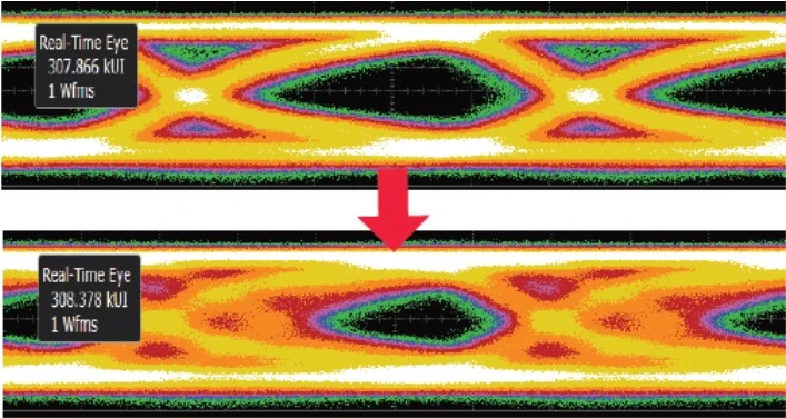
PCIe 3.0 Eye Diagram
The PCIe 3.0 standard adds the functions of receiver equalization and transmitter de-emphasis, which are critical to achieving rates of 8 GT/s and above. Equalization can be in the transmitter, the receiver, or both. PCIe 1.x and PCIe 2.x specify a simple form of equalization called transmitter de-emphasis. De-emphasis reduces the low-frequency energy received by the receiver, while equalization reduces the impact of greater channel losses at high frequencies. Receiver equalization requires various types of algorithms to be implemented, the two most common being linear feedback and decision feedback (DFE).
Transmitter de-emphasis equalization occurs at the transmitter, while DFE pre-emphasis occurs at the receiver. Receiver equalization may also include continuous time linear equalization (CTLE) in conjunction with DFE. To increase the transmission distance between the transmitter and the receiver, PCIe 3.0 introduces an active equalization adaptation process where the receiver can adjust the transmitter’s pre-spike signal and de-emphasis to achieve the equalization performance that best suits its specific transmission line. This performance requires a completely new physical layer test, namely link equalization testing of both receiver and transmitter. The purpose of the link equalization receiver test is to check if the receiver can adjust the transmitter equalization of its link under worst-case stress conditions, while the purpose of the link equalization transmitter test is to check if the transmitter performs the changes physically and logically requested by the link’s receiver.
The PCIe 4.0 standard was first introduced in 2017, providing 64 GBps throughput, doubling bandwidth while maintaining compatibility with PCIe 3.0. In addition, it strengthens channel management and error detection mechanisms and adds support for higher bandwidth requirements, such as for high-performance storage and networking applications. It wasn’t available for SSDs until 2019, though. AMD’s Ryzen 3000 series CPUs, first launched in July 2019, were the first desktop CPUs to support PCIe 4.0 x16 out of the box. For full support, users will need a new motherboard running the X570 chipset.
- PCIe 4.0
The PCIe 4.0 standard was launched in 2017, seven years after PCIe 3.0 was launched. Compared with the previous generation, PCIe 4.0 increases the transmission rate from 8 Gb/s to 16 Gb/s and is fully compatible with previous generations of technology from software to clock architecture to mechanical interface. From a protocol and encoding perspective, PCIe 4.0 has many things in common with PCIe 3.0, including 128/130-bit encoding. At first glance, PCIe 4.0 has more in common with PCIe 3.0 than PCIe 3.0 has with PCIe 2.0. However, when the speed of a device is increased, higher frequencies are automatically sent through the same channels. Insertion loss, or attenuation, is caused by resistance in the link during the transmission of electrical signals, and increases with increasing frequency.
At 16 GT/s, PCIe 4.0 signals are significantly attenuated in a typical FR4 channel (the most common printed circuit board material). Therefore, additional testing is required to ensure signal integrity in PCIe 4.0 designs because signal loss at 16GT/s (PCIe 4.0) is much greater than signal loss at 8 GT/s (PCIe 3.0). PCIe 4.0 adds a timer section to the specification to extend the range of channels and specifically increase the complexity of system testing. Even with the increased test complexity, the test times for PCIe 3.0 at 8 GT/s are higher than the test times for PCIe 4.0 at 16 GT/s. This is because PCIe 3.0 needs to test three different channel scenarios: short, medium, and long, while PCIe 4.0 only needs to test the long channel scenario.
Like PCIe 3.0, PCIe 4.0 is sometimes referred to as a “closed eyes” specification. This means that even if you have a perfect transmitter, and a transmitter with essentially zero jitter, when you connect the transmitter to a channel, the inter-symbol interference will force the “eye” to close. Whether the PCIe 4.0 signal can be successfully transmitted depends on whether the receiver’s equalization strategy can open its “eyes”. When a PCIe 4.0 device supporting 16 GT/s links to another PCIe 4.0 device supporting 16 GT/s, there are two steps to link equalization. First, the link is established at 8 GT/s, and if successful, the link equalization process is repeated once more to achieve 16 GT/s. For PCIe 4.0, designers should evaluate their system’s tolerance for performance variations. Understanding performance variations is essential because signal performance varies from card to card. These differences lead to increased channel loss, crosstalk, and channel incoherence, resulting in more system noise, degraded jitter performance, and signal eye closure.
- PCIe 5.0
The PCIe 5.0 standard was released in May 2019, bringing 128 GBps throughput while improving signal integrity and bit error rate (BER) control, and supporting higher-performance devices such as those used in artificial intelligence and high-performance computing (HPC). This specification is backward compatible with previous generations of PCIe. Intel is the first company to adopt PCIe 5.0 on its CPU, whose Alder Lake platform supports the PCIe 5.0 standard.
Since PCIe4.0, the iteration speed of PCIe has been significantly accelerated. The market of PCIe4.0 has not yet warmed up, and PCI-SIG released the PCIe 5.0 specification in May 2019, doubling the transmission rate to 32 GT/s while maintaining low power consumption and backward compatibility with previous generations. PCIe 5.0 promises 128 GB/s throughput in a x16 configuration, enabling 400GE speeds in the data center. PCIe 5.0 and 400GE speeds both support applications such as artificial intelligence (AI), machine learning, gaming, visual computing, storage, and networking. These advances are enabling innovations in 5G, cloud computing, and hyperscale data centers. The PCIe 5.0 standard is a relatively simple extension based on 4.0. It uses the same Tx and Rx test methods as PCIe 4.0, as well as similar methods for calibrating the “eye” width and height for receiver stress jitter testing.
The new standard further reduces latency and is compatible with signal loss in long-distance applications. PCIe 5.0 uses the 128b/130b encoding scheme that debuted in PCIe 3.0 and compatible CEM connectors. A new feature in PCIe 5.0 is equalization bypass mode, which enables training from 2.5 GT/s directly to 32 GT/s, speeding up link initialization. This helps reduce link startup time in systems with transmitter, channel and receiver conditions (such as embedded systems), and provides a new training path for link equalization testing at 32 GT/s. Generally, there are minor specification changes, other than where speed increases are needed, or electrical changes are implemented to improve signal integrity and the mechanical robustness of the connector.
The PCI-SIG, which defines the PCIe standard, had expected PCIe 4.0 and PCIe 5.0 to coexist for some time, with PCIe 5.0 used for high-performance needs that require maximum throughput, such as GPUs for AI workloads and networking applications. Therefore, PCIe 5.0 is predicted to be used primarily in data centers, networking, and high-performance computing (HPC) enterprise environments, while less intensive applications, such as those used by desktop computers, can use PCIe 4.0. The bandwidth of the latest PCIe 6.0 standard released in 2022 has doubled again, significantly increasing to 8 GB/s per channel, and it has also achieved huge changes in interconnection.
- PCIe 6.0
PCI-SIG released the PCIe 6.0 specification in January 2022. PCIe 6.0 technology is the first PCI Express standard to use Pulse Amplitude Modulation 4 (PAM4) signal encoding, enabling PCIe 6.0 devices to achieve twice the throughput of PCIe 5.0 devices while maintaining the same channel bandwidth. PCIe 6.0 technology can reach up to 64 GT/s while maintaining low power consumption and backward compatibility. PCIe 6.0 promises 256GB/s throughput in a x16 configuration, enabling 800GE speeds in the data center. The speed of 800GE and PCIe 6.0 jointly support applications such as AI, machine learning, gaming, visual computing, storage, and networking to promote the development of 5G, cloud computing, hyperscale data centers and other fields.
PCIe 6.0 uses the high-order modulation format PAM4 signal, which is a major upgrade to PCIe 5.0 technology. However, it uses the same high-level methodology for Tx and Rx testing while adding some new transmitter measurement encodings specific to PAM4. Similar to previous generations, PCIe 6.0 devices employ transmitter and receiver equalization for 64 GT/s operation and require forward error correction (FEC). In addition to these electrical changes, PCIe 6.0 introduces Flow Control Unit (FLIT) encoding. Unlike PAM4 at the physical layer, FLIT encoding is used at the logical layer to break data into fixed-size packets. PCIe 6.0 performs transaction transmission in units of FLIT. Each FLIT has 256 B of data (1 FLIT = 236B TLP + 6B DLP + 8B CRC + 6B FEC = 256B), and each B of data occupies 4 UI.
In addition, FLIT encoding also eliminates the 128B/130B encoding and DLLP (Data Link Layer Packet) overhead of previous PCIe specifications, significantly improving TLP (Transaction Layer Packet) efficiency. Although PCIe 6.0 has more advantages and has been proposed for more than a year, there are many uncertainties as to when PCIe 6.0 will be available to users as PCIe 5.0 has not yet been fully popularized. At present, high-performance and throughput applications require PCIe 6.0 more, such as graphics processing units for AI workloads, high-throughput network applications, and Compute Express Link (CXL) technology, which becomes the highway for data interaction under heterogeneous computing architecture. The PCIe 6.0 interface doubles the transfer rate to 64 GT/s while maintaining backward compatibility with previous generations, providing 256 GB/s throughput at the same maximum of 16 lanes.
PAM-4 electrical signal modulation scheme: Instead of using the traditional non-return-to-zero (NRZ) signal, a pulse amplitude signal with four voltage levels is used, which can produce a three-eye eye diagram. Precoding and forward error correction (FEC) can reduce analog errors and digital errors respectively. The solution can provide 64GT/s bandwidth with low latency.
Flow Control Unit (FLIT) Packet Transport: This new packet transport architecture (required by FEC) not only supports the increased bandwidth but also enables the system to handle the increased bandwidth.
L0p low power state: When bandwidth demand in the system decreases, the new L0p low power state allows some channels to enter sleep mode, thereby optimizing power consumption while ensuring that the link always remains up.
Data integrity and security protection: The specification uses Data Object Exchange (DOE) as a PCIe security building block at lower bandwidth levels and uses encrypted data and keys. Component Measurement Authentication (CMA) provides cryptographic signing of firmware. Integrity and Data Encryption (IDE) provides packet-level security for the system to prevent physical attacks. By coupling IDE with the controller, it can provide efficient security protection at a high bandwidth speed of 64GT/s.
- PCIe 7.0
After AMD first launched PCIe 4.0, Intel began to popularize PCIe 5.0 last year. Although the PCIe 6.0 specification was just announced earlier this year, the standards organization PCI SIG officially announced the development of PCIe 7.0 and previewed the core parameters. Similar to the changes in previous generations, PCIe 7.0 doubles the bandwidth again based on PCIe 6.0 to 128GT/s, and the x16 channel can reach 512GB/s in both directions. Even for the x2/x4 channels commonly used by SSDs, the theoretical peak speeds are increased to 64GB/s and 128GB/s respectively.
In terms of details, PCIe 7.0, like 6.0, uses the new PAM4 modulation and 1b/1b encoding. It is worth mentioning that PCIe 7.0 still maintains backward compatibility. The PCI SIG organization stated that the next draft will focus on optimizing channel parameters and improving energy efficiency. According to the plan, the PCIe 7.0 standard will be completed in 2025, and it is believed that it will not be fully popularized until around 2028; Although we are making every effort to promote new technologies, I would like to ask a question: how long will it take before we see PCIe 6.0 products officially released?